Continue to Site

Welcome to EDAboard.com

Welcome to our site! EDAboard.com is an international Electronics Discussion Forum focused on EDA software, circuits, schematics, books, theory, papers, asic, pld, 8051, DSP, Network, RF, Analog Design, PCB, Service Manuals... and a whole lot more! To participate you need to register. Registration is free. Click here to register now.

Shielding PCB with DGND?

Status
Not open for further replies.

digi001

Full Member level 5
Joined
Apr 5, 2011
Messages
244
Helped
22
Reputation
44
Reaction score
21
Trophy points
1,298
Activity points
2,904
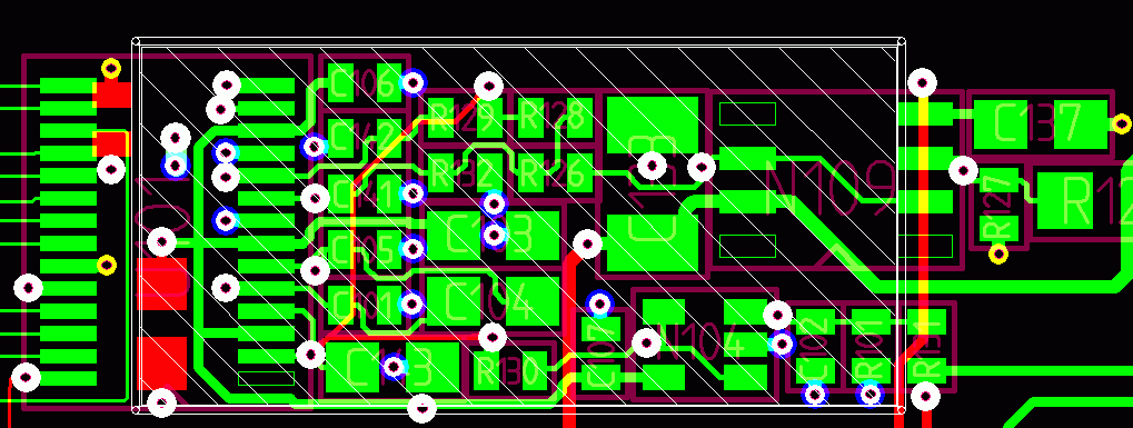
-8 Layer PCB (10 if add Shield) with DSP/4xADC/4xDAC/FPGA and more. Populated top and bottom. +15,-15V with AGND///+5V with DGND

Located in very noisy environment near power supplies etc.

Good idea or bad idea to Shield with DGND on Top & Bottom for noise immunity?
 
Last edited:

You could reserve TOP and BOTTOM, in order to shield signals inside that layers 'sandwich'.
Other important arrangement, is to insert GND vias as much as possible, crossing and connecting all layers.

+++
 
  • Like
Reactions: digi001

    digi001

    Points: 2
    Helpful Answer Positive Rating
I would suggest that you would be very cautious on pouring this DGND onto your top and bottom layer by not overlapping DGND and AGND together, or extending your DGND to analog area which may pollute your AGND eventually.
 
  • Like
Reactions: digi001

    digi001

    Points: 2
    Helpful Answer Positive Rating
you may add shielding can for space noise and damage;
 

Curious, if you have 4 ADC, 4 DACs, how are you connecting your AGND and DGND? how are the planes seperated etc. Done a few designs with multiple ADC/DAC codecs FPGA's DSP and use only ONE Ground.
As to shielding, first stop, Henry Ott and the compliance club.
home page
EMC Information Centre - The EMC Journal (Free in the UK)
 
  • Like
Reactions: digi001 and FvM

    FvM

    Points: 2
    Helpful Answer Positive Rating

    digi001

    Points: 2
    Helpful Answer Positive Rating
AGND And DGND Planes are separated now and tied in the corner of the board with a Jumper.
 
Last edited:

A possible EMC nightmare. Dont take this wrong, but I think that your stack up and seperation of the grounds is going to cause you problems. What signals are going to be routed on Signal3 and signal4. Have you thought about the loop around the board to the corner join of the AGND and DGND planes. What power will be distributed on the second power layer. Vias are going to couple planes together. You should not overlap any AGND and DGND planes if you are going to split them, you should not route any digital signals over the AGND plane, and having a join in a corner add extra loops. Hvae a look at the DACs and ADCs the AGND and DGND is connected inside the chip quite often, so there are numerous unconbtroleed and different length loops created. The small high impedance link joining the AGND and DGND planes will cause the planes to lift if EMI noise is picked up, which it probably will be, causing the convertors to loose resolution.

http://www.hottconsultants.com/techt...gnd-plane.html
**broken link removed**
An intuitive, practical approach to mixed-signal grounding
**broken link removed**
http://focus.ti.com/lit/ml/slyp167/slyp167.pdf
http://www.ieee.org.uk/docs/emc1206a.pdf
**broken link removed**
 
Done a few designs with multiple ADC/DAC codecs FPGA's DSP and use only ONE Ground.
It's always funny to read datasheets recommending separate grounds. Of course they have to be connected directly at the respective chip... :)

Seriously speaking, separated grounds are good for high dynamic, low frequency applications or power electronics. RF and high frequency mixed signal would usually go for continuous ground planes, closely tied together, and faraday cages to deal with EMC. In special cases, you may want to have part of a circuit using a separate ground, But then no fast signals should cross their boundary.
 
  • Like
Reactions: digi001

    digi001

    Points: 2
    Helpful Answer Positive Rating
Again when you have more than one device you cannot have a single star point. From the informations out there (and I have LOTS regarding seperate grounds) and from past experience, ONE contigous ground is best. What you do have to do is carry out very fastidous component placement and routing, and in some cases have to seperate the boards to get the best results (high power designs, motor controllers etc). If you do have to add splits to create a seperate ground area do so as shown in link below, and then only if you know what you are doing.
Grounding of Mixes Signal Systems
Slots in Ground Planes
And finaly the Ground (0V, return plane etc etc) is Lord of the board:::
**broken link removed**

Sorry, I'll take a calm down pill now, but I have found seperate grounds, engineers differing views on grounding and trying to guestimate where the returns are going, especially when you add EMC effect into the equation has caused me more problems, than having one contigous ground and letting the currents sort them selves out.
Exception to this are high power, SMPS etc, but here I employ what I call strategic ground partitioning, which involes coloured pencils (to plan the returns) and lots of work. I have been doing boards for 25 years and have studied Ground/return paths for all that time, and have seen numerous trends and views change regarding the return paths. But these days with the aboundance of SMPS, HVAC high speed digital, wireless communications etc, you have to factor in possible EMC problems along with increased digital rise time, lower chip voltages etc etc and so one ground is best.
Historicly when I first started doing ADC and DAC boards, logic was slower (Rt and clock frequencies), packages were bigger, the analogue section often worked at +/-15V and you could get away with seperate AGND and DGND. Now with the ever decreaing size of devices, reduced working voltages and densly packed designs it is more problematic to try and seperate the grounds without creating either multiple loops (star point loops) or the star point creating effectively a huge ground plane split and the added noise that creates, as said often wiping out the lower bits of a convertor.
:grin:

It was working on this project that realy got me interested in grounds, and how critical they are.
http://accelconf.web.cern.ch/accelconf/e94/PDF/EPAC1994_1551.PDF
 
  • Like
Reactions: digi001

    digi001

    Points: 2
    Helpful Answer Positive Rating
Several years ago, I did an experiment to keep the idea of separate analog grounds in a mixed signal design with multiple 50 MHz 12 Bit ADCs. Following the recommendation to connect it under the ADC, I used individual analog planes for each ADC and it's related pre amplifier, as shown below. The white split plane is the analog ground, the digital ground plane is continuous. The design basically worked, but unfortunately, the open end of analog plane (at the right side) is carrying huge EMI levels, stimulated by the single ended ADC clock and output data signals.

That's been the last time I used separated grounds for high speed mixed signal design.

 
  • Like
Reactions: digi001

    digi001

    Points: 2
    Helpful Answer Positive Rating
Power in my system is +15,-15V which return to AGND and +5V which returns to DGND
 

Some devices will connect to both analog and digital signals and possibly inject differential currents between both ground nodes. To understand the effect of using separate grounds in your design, we would need to analyze the impact of ground voltage differences and the return path for injected currents in each case. At best, it won't harm and not cause interferences exposed to the outside.
 

Not only that, but whatever signals are on Signal3 will use the AGND plane as there return path, and will also capacitively couple to that plane, the return for these currents is going to have to travel a torturous path along the plane, through your corner link and back to the source.
Again as FvM has said, you cannot guarantee what is going to use what plane as a return, hence careful sgregation of the various sections and where the traces run, with one ground.
The older style chips were more benign for split planes, but with a lot of modern devices in QFN 0.5mm pitch, and the proliferation of numerous devices on a board it just gets more problematic.
 
  • Like
Reactions: digi001

    digi001

    Points: 2
    Helpful Answer Positive Rating
Curious, if you have 4 ADC, 4 DACs, how are you connecting your AGND and DGND? how are the planes seperated etc. Done a few designs with multiple ADC/DAC codecs FPGA's DSP and use only ONE Ground.
As to shielding, first stop, Henry Ott and the compliance club.
home page
EMC Information Centre - The EMC Journal (Free in the UK)

Yes I am learning that 1 ground may be more appropriate for this design (as we have some noise issues with 2 ground design).

---------- Post added at 08:49 ---------- Previous post was at 08:47 ----------

Found this article in another thread that actually helped to solve some of our issues:

Analog Devices: Analog Dialogue: Ask The Applications Engineer - 12
 

Glad your getting results, this was what we found happening, but back then 2004/5 to mention having one ground was heretical talk almost. Even now some are hard to convince, but I persevere.:grin:
Been a fun discussion thanks Templemark and of course FvM
 

Yes thanks for all the responses!

I may have to start a new thread about another PCB GND Topic

---------- Post added at 16:11 ---------- Previous post was at 15:23 ----------

A possible EMC nightmare. Dont take this wrong, but I think that your stack up and seperation of the grounds is going to cause you problems. What signals are going to be routed on Signal3 and signal4. Have you thought about the loop around the board to the corner join of the AGND and DGND planes. What power will be distributed on the second power layer. Vias are going to couple planes together. You should not overlap any AGND and DGND planes if you are going to split them, you should not route any digital signals over the AGND plane, and having a join in a corner add extra loops. Hvae a look at the DACs and ADCs the AGND and DGND is connected inside the chip quite often, so there are numerous unconbtroleed and different length loops created. The small high impedance link joining the AGND and DGND planes will cause the planes to lift if EMI noise is picked up, which it probably will be, causing the convertors to loose resolution.

http://www.hottconsultants.com/techt...gnd-plane.html
**broken link removed**
An intuitive, practical approach to mixed-signal grounding
**broken link removed**
http://focus.ti.com/lit/ml/slyp167/slyp167.pdf
http://www.ieee.org.uk/docs/emc1206a.pdf
**broken link removed**

marce: a few of these links dont work for me because of the "..." in them. Could you possibly fix this with the right link? Great Links!
 

Over a DVD worth of documents regarding PCB Layout Design??
 

I would like to share my point of view of why most of the people didn't want to go for single plane, as for my case, they would think that analog circuit will be polluted by digital circuits by having the same contiguous ground. But they have miss out the point that by proper segregration of circuit, and visualizing it using EM waves when signals travel down the trace, of course with continuous reference right below the trace, they are no reason for the digital signals to haphazardly extend its wave to pollute the analog circuits, since EM wave is tightly coupled to the reference plane below during high speed operation. Splitting of plane just increases the risk of having uncontrolled return path in this case.
 

I am lucky in that I do a job I realy do enjoy, PCB Design. I am into all aspects of it from the Layout , Signal Integrity, EMC to the manufacturing and assembly side. I started around 1985 using then Redboard (Cadstar pre-cursor) but also 'red and blue' tape ups. In fact as the 'junior' PCB guy when I started I did mainly the tape ups for the first 9 months. This was an excelleny education as with tape ups mistakes are costly, so you learned to see the patterns of routes in your head from the schematic (no rubber banding connections to guide placement). I have also worked closely with production departments on all aspects of PCB assembly and packaging the final product.
Because there are so many facets to PCB design, you never get bored, and there is always somthing new to learn and study, even now after so many years, I still have so much to learn. The more I study a paticular aspect of design the more I find to I have to learn.
Another set of documantation that I believe any organisation should have, that are designing PCBs is this collection from the IPC, I have mine on the desk ready for instant access.
https://portal.ipc.org/Purchase/ProductDetail.aspx?Product_code=4499ABA8-7C32-DD11-A3F8-001422202D38
 

Status
Not open for further replies.

Part and Inventory Search

Welcome to EDABoard.com

Sponsor

Back
Top