seridj_mse
Member level 2
dear experts ,
After a hard #work to reduce noise for certify our equipment directive CISPR 16-2-3 class B with LNE , i had basically tow problem :
1- harmonics 50 MHz oscillator for Ethernet 10/100M design in mother boar. that is not the point of this post.
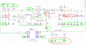
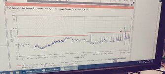
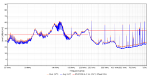
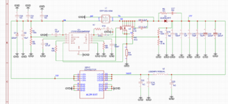
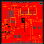
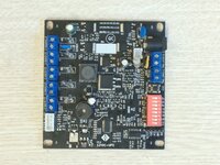
2- noise in power supply of our mother board we use a SEPIC DC DC converter 24w large input 9-30v and fixe output 12v@2A. for conducted emissions it was good but for radiation emissions it was very Noisy
  so I started dig into the issue and what is the source of this noise, hot loop as small as possible
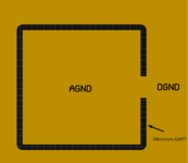
 , ground MOSFET as close as possible to gnd output capacitor, change référence of components with better intrinsic characteristics change PCB placement and layers .... keeping in the mind
  the price of those changes
  and the most important thing the right functioning of the board
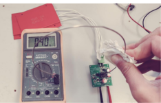
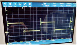
So now i can say i was very successful reduce noise but when i measured temperature of components, the surprise
 :
:
-Before modification at max load 2A :
- Coupled inductor : 49°
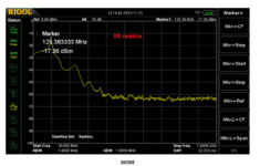
- Diode : 55°
-Mofet : 45°
After modification :
- Coupled inductor : 64°
- Diode : 68°
- Mosfet :77°
Note : i take those measurements with my old multimeter and K probe thermometer
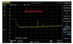
So maybe i know why i use a 50R for gate Mosfet so i think
  i should find another method like use 4 layers PCB.
TO YOUR KEYBOARD for any help
After a hard #work
to reduce noise for certify our equipment directive CISPR 16-2-3 class B with LNE , i had basically tow problem :1- harmonics 50 MHz oscillator for Ethernet 10/100M design in mother boar. that is not the point of this post.
2- noise in power supply of our mother board we use a SEPIC DC DC converter 24w large input 9-30v and fixe output 12v@2A. for conducted emissions it was good
but for radiation emissions it was very Noisy so I started dig into the issue and what is the source of this noise, hot loop as small as possible, ground MOSFET as close as possible to gnd output capacitor, change référence of components with better intrinsic characteristics change PCB placement and layers .... keeping in the mind the price of those changes and the most important thing the right functioning of the board So now i can say i was very successful reduce noise
but when i measured temperature of components, the surprise :-Before modification at max load 2A :
- Coupled inductor : 49°
- Diode : 55°
-Mofet : 45°
After modification :
- Coupled inductor : 64°
- Diode : 68°
- Mosfet :77°
Note : i take those measurements with my old multimeter and K probe thermometer
So maybe i know why
i use a 50R for gate Mosfet so i think i should find another method like use 4 layers PCB.TO YOUR KEYBOARD for any help
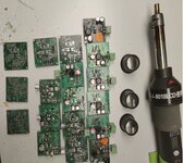
Attachments
Last edited:
") Every design need a balancing, with higher frequency has more advantages than low frequency, but the "balance point" has more to do.
Every design need a balancing, with higher frequency has more advantages than low frequency, but the "balance point" has more to do.