Continue to Site

Welcome to EDAboard.com

Welcome to our site! EDAboard.com is an international Electronics Discussion Forum focused on EDA software, circuits, schematics, books, theory, papers, asic, pld, 8051, DSP, Network, RF, Analog Design, PCB, Service Manuals... and a whole lot more! To participate you need to register. Registration is free. Click here to register now.

Sampling switch uses a bootstrapping technique

Status
Not open for further replies.

shuy

Newbie level 4
Joined
Nov 14, 2022
Messages
7
Helped
0
Reputation
0
Reaction score
0
Trophy points
1
Activity points
66
hi all,
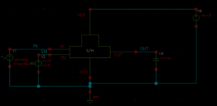
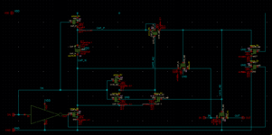
As part of the ADC design project, I designed a switch based on bootstrapping technique. I would appreciate help regarding the function of the transistor M10. It seems to work in parallel with M7 so it can be omitted.
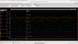
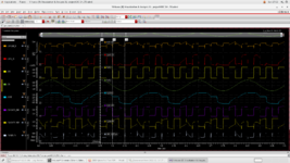
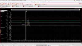
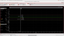
After simulations in Virtuoso, I saw that the circuit functions even better without it.
Thank you
צילום מסך_20221114_135755.png
 

I wouldn't remove it. M7 source is connected to the input signal while the gate is at fixed Vdd. So, the Ron of M7 will vary with the signal and will modulate the Ron of M2. M10 has more or less fixed Vgs,
In order ot have the bootstrapping action you need to pull the gate of M2 down to turn it off. At the end of the charging phase the source of M7 is for a short time at gnd and it pulls the gate of M2 down. Then M10 takes over.
 

Thank you for your reply,
Is the case you describe valid only for input voltages greater than Vdd-Vt? Otherwise, m7 alone is enough.
 

Thanks again.
I am attaching a simulations of input voltage from 0 to VDD with and without M10.
No difference is seen in the output voltage for dc input, and for ac the output voltage more accurate without m10.
Can you tell me for which input voltages the circuit will not work without m10?
 

Attachments

  • Screenshot from 2022-11-14 12-38-42.png
    Screenshot from 2022-11-14 12-38-42.png
    14.5 KB · Views: 123
  • no m10.png
    no m10.png
    224 KB · Views: 122
  • with m10.png
    with m10.png
    222.8 KB · Views: 116
  • with m10 2.png
    with m10 2.png
    197.2 KB · Views: 114
  • no m10 2.png
    no m10 2.png
    191.8 KB · Views: 118
  • Screenshot from 2022-11-14 12-35-33.png
    Screenshot from 2022-11-14 12-35-33.png
    38.1 KB · Views: 136

Connections on the M6/M7 transistors from schematic posted on #5 do not matches to the original circuit posted on #1
 

i cant see the difference, you can explain it for me?
Read M7/M10 where I wrote M6/M7.
Note that you connected the M7 gate net to the M10 gate and body nets on your implemented circuit.

M6_M7.png
 

Thanks again.
I am attaching a simulations of input voltage from 0 to VDD with and without M10.
No difference is seen in the output voltage for dc input, and for ac the output voltage more accurate without m10.
Can you tell me for which input voltages the circuit will not work without m10?
since you have all the simulations, can you tell me what pulls the gate of M2 low and the gate of M10 high right after your clock goes high?
 

since you have all the simulations, can you tell me what pulls the gate of M2 low and the gate of M10 high right after your clock goes high?
During track mode, ’sn’ is high and transistor M7 turns on. as a result, transistor M2 opens and forces Vdd on transistor M5 gate, consequently, the positive plate of the MOS capacitor connects to the gate of M0 (same gate like M10) and the negative plate connects to the input voltage so its gate potential is equal to the source voltage plus the supply voltage (Vdd). Thus, the Vgs of transistor M0 is equal to Vdd, and, therefore, its resistance, is independent of the input voltage.

Read M7/M10 where I wrote M6/M7.
Note that you connected the M7 gate net to the M10 gate and body nets on your implemented circuit.

View attachment 179743
'sn' push M7 gate, I connected only the bulks of M7, M10 to gnd.
 

During track mode, ’sn’ is high and transistor M7 turns on. as a result, transistor M2 opens and forces Vdd on transistor M5 gate, consequently, the positive plate of the MOS capacitor connects to the gate of M0 (same gate like M10) and the negative plate connects to the input voltage so its gate potential is equal to the source voltage plus the supply voltage (Vdd). Thus, the Vgs of transistor M0 is equal to Vdd, and, therefore, its resistance, is independent of the input voltage.
From your simulation, if I see this correctly you don't have Vgs of Vdd on M0. Could there be a problem on node Cap_p shouldn't it go higher Vdd+vin and not only as in your simulation to around 5.6 V.
 

During track mode, ’sn’ is high and transistor M7 turns on. as a result, transistor M2 opens and forces Vdd on transistor M5 gate, consequently, the positive plate of the MOS capacitor connects to the gate of M0 (same gate like M10) and the negative plate connects to the input voltage so its gate potential is equal to the source voltage plus the supply voltage (Vdd). Thus, the Vgs of transistor M0 is equal to Vdd, and, therefore, its resistance, is independent of the input voltage.


'sn' push M7 gate, I connected only the bulks of M7, M10 to gnd.

So, you are confirming what I said in my first comment in #2 that right after sn goes high it is the M7 that pulls down the gate of M2, after which M10 takes over.
Now, if you remove M7, what will pull the gate of M2 down initially?
 

From your simulation, if I see this correctly you don't have Vgs of Vdd on M0. Could there be a problem on node Cap_p shouldn't it go higher Vdd+vin and not only as in your simulation to around 5.6 V.
From the theoretical analysis there should indeed be Vin+Vdd at the gate of M0, but in practice there is a voltage drop as a result of charges that open M5, M0 or leak through M3.

So, you are confirming what I said in my first comment in #2 that right after sn goes high it is the M7 that pulls down the gate of M2, after which M10 takes over.
Now, if you remove M7, what will pull the gate of M2 down initially?
I agree that M7 is critical to circuit function. I opened the discussion regarding the role of M10. I think M7 alone can do the trick. (The simulations are also with and without M10)
 

From the theoretical analysis there should indeed be Vin+Vdd at the gate of M0, but in practice there is a voltage drop as a result of charges that open M5, M0 or leak through M3.


I agree that M7 is critical to circuit function. I opened the discussion regarding the role of M10. I think M7 alone can do the trick. (The simulations are also with and without M10)
Yes it won't reach exactly Vin+Vdd but only 5.6 is way to low your problem is M3 when the drain voltage goes above Vdd your bulk is below the drain Voltage and the drain bulk diode opens that is also the reason you don't see the effect of M10 because M5 doesn't open fully and node C_n is less than Vin. You need M10 for high input Voltages when the node C_n is vdd-vth and M7 shuts off and the gate of M2 starts floating this prevents M10 as he takes over and pulls the gate of M2 to vin.
 

Yes, exactly. Bulk of M3 has to be connected to CAP_P. And correctly stated that M7 won't turn on when having high input voltages because its gate is at VDD.
 

Yes it won't reach exactly Vin+Vdd but only 5.6 is way to low your problem is M3 when the drain voltage goes above Vdd your bulk is below the drain Voltage and the drain bulk diode opens that is also the reason you don't see the effect of M10 because M5 doesn't open fully and node C_n is less than Vin. You need M10 for high input Voltages when the node C_n is vdd-vth and M7 shuts off and the gate of M2 starts floating this prevents M10 as he takes over and pulls the gate of M2 to vin.
I agree about connecting the body of the M3 transistor to the source. Regarding the role of the M10 transistor, this was my theory, but as you can see from the simulation for Vin=Vdd=5V>Vdd-vt is still obtained at the output Vout=5v even without the M10 transistor.
 

Status
Not open for further replies.

Part and Inventory Search

Welcome to EDABoard.com

Sponsor

Back
Top