Continue to Site

Welcome to EDAboard.com

Welcome to our site! EDAboard.com is an international Electronics Discussion Forum focused on EDA software, circuits, schematics, books, theory, papers, asic, pld, 8051, DSP, Network, RF, Analog Design, PCB, Service Manuals... and a whole lot more! To participate you need to register. Registration is free. Click here to register now.

sample hold circuit help

Status
Not open for further replies.

prcken

Advanced Member level 1
Joined
Nov 1, 2006
Messages
419
Helped
41
Reputation
82
Reaction score
37
Trophy points
1,308
Location
Shanghai
Activity points
4,059
photo.JPG
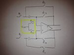
please have a look at this SH schematic, the wired thing is that I have to connect vcm at phase 1a to the differential input to make it operational. in theory it should work without that Vcm to inputs at 1a phase, for it is in feedback configuration at phase 2, the input common mode is set in the opamp itself with CMFB.

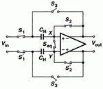
I checked some previous discussion in eadboard, even i tried with Seq switch in Razavi's book as below, it's still not functional.
7_1220565783.gif
because that Seq switch is intended for mitigate mismatch, here is seems not the mismatch problem. and seems not charge injection issue, either, because i tried to use ideal switches.

any ideas and comments ?

Thanks!
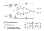
 

This is commonly know as Flip around S/H structure .The circuit should work if you use non-overlapping clocks and charge injection will only result in error voltage at the output but the output will surely come as required .
 

This is commonly know as Flip around S/H structure .The circuit should work if you use non-overlapping clocks and charge injection will only result in error voltage at the output but the output will surely come as required .
thanks for your reply. Yes, in theory, it should work. but in practical, at higher sample rate, not easy to make it work well as you wanted.
i found another method to bias the opamp in open loop way, in which [Ishii, H., K. Tanabe, and T. Iida. A 1.0 V 40mW 10b 100MS/s pipeline ADC in 90nm CMOS. in Custom Integrated Circuits Conference, 2005. Proceedings of the IEEE 2005. 2005.] the input common mode can be set as whatever you want, not set by the output common mode.
Capture.PNG
 

What is you sampling rate ?And having an opamp in openloop is really not good in practical situations .it is advicasble to have it in closed loop always .can you post the i9mages of the i/p and o/p waveforms you are getting ?
 

What is you sampling rate ?And having an opamp in openloop is really not good in practical situations .it is advicasble to have it in closed loop always .can you post the i9mages of the i/p and o/p waveforms you are getting ?

Yes, I agree.
but when the opamp in consecutive MDACs is shared in pipelined ADC, it can't be biased by feedback. anyway, for SHA it can!
I designed a SHA running at 50MHz sampling rate less ringing weeks ago, but didn't really do optimization. now, i am really trying to do optimization for it, it rings a lot, it's so weird and really frustrating.
below is my previous design w/o optimization with feedback bias scheme. 50MHz sampling clock, 5MHz input sine wave, 1.2 Vpp differential output and output common mode signals
Capture.PNG
Now the new design is messed up.
 
Last edited:

just for confirming -Are you using nonoverlapping clocks ????
and also if you are using this ckt in cadence ,are you using ideal components ???
and if so what library are you using ??
50MHz is small frequency if we design the opamp designed is good ....
 

just for confirming -Are you using nonoverlapping clocks ????
and also if you are using this ckt in cadence ,are you using ideal components ???
and if so what library are you using ??
50MHz is small frequency if we design the opamp designed is good ....
Yes, I am using ideal non-overlapping clocks. that waveform i posted was got from all transistors including switches. and also i designed first with ideal switches from analogLib.
I think it's the opamp messed up.
 

Is the opamp you are using a ideal one? Can u post a pictures of your cadence circuit.the output seems be wrong .when you sample a sine wave you might get a different output if your opamp doesn't reset.normally to reduce ringing we reduce the phase margin of it to get smoother output
 

Is the opamp you are using a ideal one? Can u post a pictures of your cadence circuit.the output seems be wrong .when you sample a sine wave you might get a different output if your opamp doesn't reset.normally to reduce ringing we reduce the phase margin of it to get smoother output

of course not ideal opamp, i that waveform got from the loop spec. Phase margin of 53 degree and funity of 153MHz.
it's a two stage opamp operating at 1.2V power supply, first stage folded cascode with class AB second stage
 

well the opamp has good PM ....can u use a single stage instead of 2 stage amp ......is there a specific reason for using 2 stages like o/p swing???what is the gain you are aiming at ???
ths S/H gets reset every cycle after transfer of charge ......can you use a S/H which doesnt do that ....there are many such structures available in the books ....the structure you are using sets the o/p to Common mode after every cycle which is not good for the opamp which is why ringing is occuring .....if you have flexibility of choosing a different structure pls use one which doesnt do that ...the opamp will have lesser things to process ..
 
Last edited:

well the opamp has good PM ....can u use a single stage instead of 2 stage amp ......is there a specific reason for using 2 stages like o/p swing???what is the gain you are aiming at ???
ths S/H gets reset every cycle after transfer of charge ......can you use a S/H which doesnt do that ....there are many such structures available in the books ....

single stage will use gain boosted topology, and swing is smaller, here for 1Vpp folded cascode seems also can meet the swing spec. i am not 100% sure how to define the gain of the opamp in pipleline ADC. for the 1st stage, let's say the static gain error ε is approximately 1/(βA) , β is the feedback factor, how to define the ε?
if i set ε to be (LSB/2)/(Vpp/2) , which is 0.195% for Vpp=1V, 10-bit, 57dB gain is required, if i set ε to be 0.1%, 61dB gain is required. what's more, i found the loop gain drops by using PSS & PSTB simulation comparing to STB with ideal (continuous time) CMFB.

untitled.PNG
see the top level of the simulation schematic, you said SH o/p desn't reset, i think only need a pair of switch before the load cap, which will belong to the next stage in the pipeline
 

well the opamp has good PM ....can u use a single stage instead of 2 stage amp ......is there a specific reason for using 2 stages like o/p swing???what is the gain you are aiming at ???
ths S/H gets reset every cycle after transfer of charge ......can you use a S/H which doesnt do that ....there are many such structures available in the books ....the structure you are using sets the o/p to Common mode after every cycle which is not good for the opamp which is why ringing is occuring .....if you have flexibility of choosing a different structure pls use one which doesnt do that ...the opamp will have lesser things to process ..

- - - Updated - - -


- - - Updated - - -

i have used the following MDAC for a pipelined ADC at 80MHz ....it shud work properly ....pls take a look into the structure mdac.png

- - - Updated - - -

if you have any doubts let me know ...its simple mdac strucure i used for 12 bit ADC....
 

thanks.
i don't understand " the structure you are using sets the o/p to Common mode after every cycle which is not good for the opamp which is why ringing is occurring"
i think that's the way CMFB works, the o/p should go back to the output common mode level.
is that ideal opamp in the schematic you posted?
 

yeas that was an ideal opamp......i would like you to answer one question for me .....isnt it enough if the i/p CM for opamp is set ,should you always short the o/p to CM after every cycle ....
i have this idea..first the cap samples ,at this time just connect the i/p to the o/p thus having the opamp o/p and i/p shorted .......
2nd phase-the cap is flipped around and this volatge is copied onto your output .....and in the next phase the similar thing of o/p shorting the i/p is repeated .......
do you really need to set the o/p to CM every cycle ???

well, ideal opamp is another thing, not hard. it did one running at 100MHz sampling rate.
real opamp needs CMFB to well define the differential output common mode voltage, it should not be set by the input common mode, instead, the input common mode is easy and flexible, in my opinion.
 

well i will design an opamp and will post the results for u tomm ....i will build a S/H using it and will post the result tomm
 

well i will design an opamp and will post the results for u tomm ....i will build a S/H using it and will post the result tomm

how is going? had fun with the opamp design? :)
 

Status
Not open for further replies.

Similar threads

Part and Inventory Search

Welcome to EDABoard.com

Sponsor

Back
Top