Continue to Site

Welcome to EDAboard.com

Welcome to our site! EDAboard.com is an international Electronics Discussion Forum focused on EDA software, circuits, schematics, books, theory, papers, asic, pld, 8051, DSP, Network, RF, Analog Design, PCB, Service Manuals... and a whole lot more! To participate you need to register. Registration is free. Click here to register now.

About Sample & Hold circuit

gagagagazi

Newbie
Joined
Dec 14, 2022
Messages
3
Helped
0
Reputation
0
Reaction score
0
Trophy points
1
Activity points
47
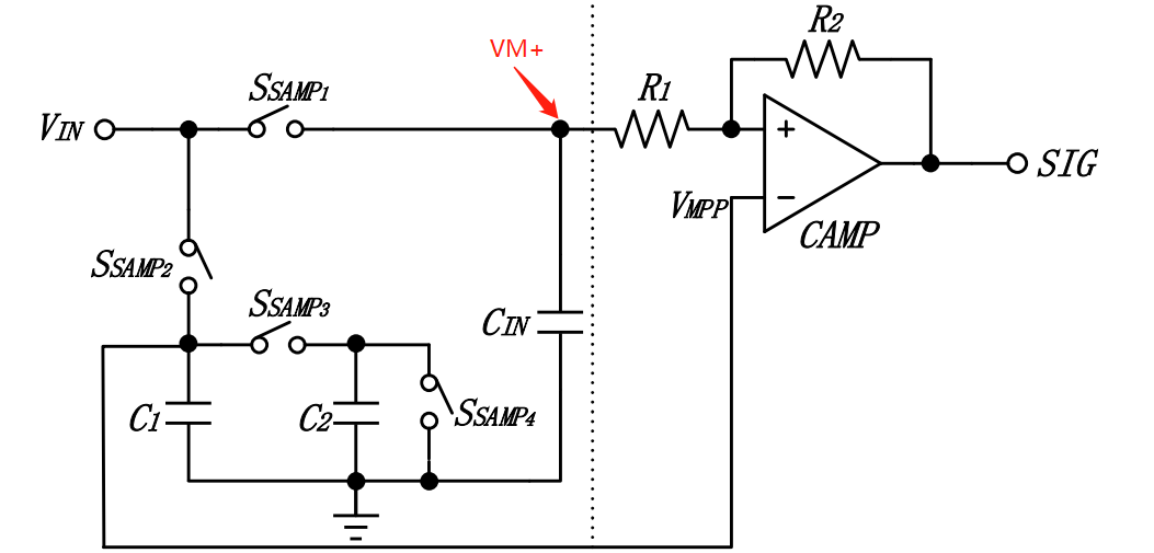
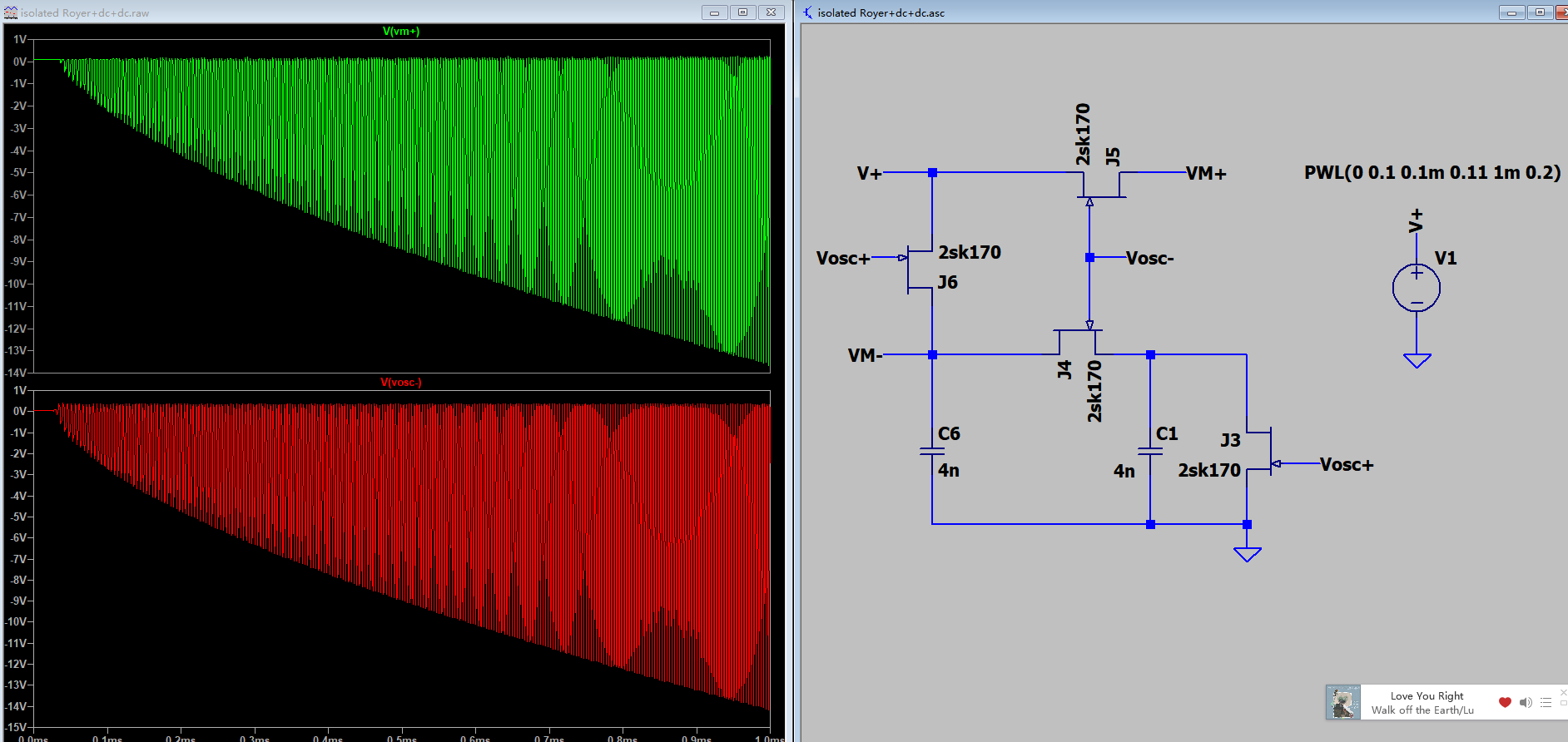
I am trying to study a Sample&Hold Citcuit, as shown in Fig.1, Vosc- and Vosc+ are the signals (opposite signals) that control J3~J6 generated by the pluse generator respectively, and the in Fig.2, my understanding It is when J4 and J5 are closed at the same time, the voltage of point VM+ should be the input voltage V+, but I don't know why, when I simulated in LTspice, the voltage of VM+ is almost the same as the signal Vosc- (as shown on the left side of Fig.1), I don't know what caused this, is there any solution? Thank you so much.
1693236888261.png

Fig.1
1693236994982.png

Fig.2
 
Switch phasing must ensure there is no overlap which
would ohmically mess up the transfers-of-charge.

4nF is pretty chubby. Maybe FET on resistance makes
a time constant that is lower than your sampling pulse
pulse width and so incapable of a clean single pulse
sample. Zoom in on a single clock cycle and assess
the sampling settling, and the hold droop.

But how you expect to control -15V signal with FETs
operating between Gnd and positive supply, I do not
see offhand. Maybe you should back up a few steps
and figure out the regions where those FETs have
actual, proper authority / operation - including that the
controlling sources are doing the right thing at those
various bias-points.
 

LaTeX Commands Quick-Menu:

Similar threads

Part and Inventory Search

Welcome to EDABoard.com

Sponsor

Back
Top