Continue to Site

Welcome to EDAboard.com

Welcome to our site! EDAboard.com is an international Electronics Discussion Forum focused on EDA software, circuits, schematics, books, theory, papers, asic, pld, 8051, DSP, Network, RF, Analog Design, PCB, Service Manuals... and a whole lot more! To participate you need to register. Registration is free. Click here to register now.

S-parameters for cirquit with lumped component in Momentum

Status
Not open for further replies.

Gigan

Member level 1
Joined
Feb 26, 2006
Messages
41
Helped
1
Reputation
2
Reaction score
1
Trophy points
1,288
Activity points
1,596
S-parameters for circuit with lumped component in Momentum

I have a question:

Is it possible in ADS Momentum to simulate directly the
S-parameters of the circuit containing lumped components (amplifier chip, smd resistors, capacitors, the amplifier has a s2p Touchstone file from the manufacturer).

If not, which EM simulation software can do?
Please answer
 

Not directly.
But you can connect these components in a seperate schematic view to simulate.( EM Co-Simulation)
 

Not directly.
But you can connect these components in a seperate schematic view to simulate.( EM Co-Simulation)

Do you remember/can show some simple example?
 

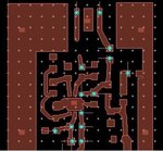
The DXF file was imported and opened in ADS Layout. Design was simplified (cleaned) temporarily - to build a simple layout co-simulation. There is only top conductor layer in it (See Photo).
But ADS assigned to him the wrong layer number Nr3 with name "resi" instead of Nr1 with name "cond" .
I decided to copy the drawing of the "resi" in to layer "cond" and then delete the layer "resi"...

but - can not copy or move shape from one layer to the other ...
I tried to copy-paste as well as the commands of the ads AEL: de_copy_to_layer ();
but ADS writes: ... there is no such command ...
the command de_move_to_layer (); is not working too.
(Two previous commands of the copy process : de_select_all (); de_set_layer (); - are working good.)


Are there any ideas, experiences, how to prepare the correct layer?
please tell !

- - - Updated - - -

OK. This (copy) problem is solved.
 

Attachments

  • Layer_resi.jpg
    Layer_resi.jpg
    291.3 KB · Views: 116

The DXF file was imported and opened in ADS Layout. Design was simplified (cleaned) temporarily....

for an exercise in co-simulation a simple layout 2-layer, consisting of only the top layer (of complete design) and Gnd level has been created. FR4 thickness is about 1.5mm. (See. Photo 1).

then the corresponding layout-component was created, and placed in the schematic window ...
it looks the co-simulation (in the schematic window) works ...

Now I would like to make a parametric sweep of the dimension L of a small strip separately ...
(Top right corner on Pic2) and to see the S-parameters changing as function of the size.
To do this - i am trying to reduce partially the size of one strip, and instead of it - to insert a MLIN of the same size with the hope to create a variable (var=L)...

questions:
1.) after reducing of the strip - its "frame" remains (see Photo 2));
how to fix it?
2) whether it is possible to replace part of layout by MLIN (or by others.)?
if so, how to create var (of length L)?
probably in the schematics?

- - - Updated - - -
 

Attachments

  • Photo2.jpg
    Photo2.jpg
    226 KB · Views: 98
  • Photo_1_1.jpg
    Photo_1_1.jpg
    43.6 KB · Views: 103

questions:
1.) after reducing of the strip - its "frame" remains (see Photo 2));
how to fix it?

Don't worry - this is the display of the previous Momentum mesh. You can clear it with EM > Clear Momentum Mesh.

2) whether it is possible to replace part of layout by MLIN (or by others.)?
if so, how to create var (of length L)?

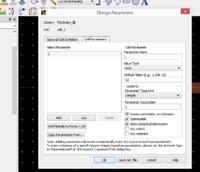
You can create a design parameter for your subcircuit (File > Design Parameters > Cell Parameters) and use that to control the MLIN parameters.

Or instead of using MLIN, you could also create an EM parameter (EM > Component > Parameters) with the "graphical" geometry stretching. Details can be found in the ADS help document. From my experience, this way to parameterize your layout can be tricky because it creates AEL layout code behind the scenes that draws AEL artwork instead of the initial geometry.
 
  • Like
Reactions: Gigan

    Gigan

    Points: 2
    Helpful Answer Positive Rating
Don't worry - this is the display of the previous Momentum mesh. You can clear it with EM > Clear Momentum Mesh.
....

Thank you Volker for great "tips"...
I used ADS earlier, several years ago...

Could you please explain also how to put few vias to ground in easiest way?
 

Could you please explain also how to put few vias to ground in easiest way?

Draw a shape (round or square or whatever you want) in layout on a layer of your choice (e.g. "holes") and map that layer in the Momentum substrate as a via between the "cond" layer and the bottom ground boundary.

For via fences, you can use Edit > Copy/Paste > Step and Repeat ...
 
  • Like
Reactions: Gigan

    Gigan

    Points: 2
    Helpful Answer Positive Rating
Hi Volker,
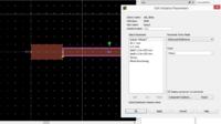
I am trying to make the length of MLIN as variable (see photo1) using your first method (File > Design Parameters > Cell Parameters).
I am doing something wrong by assigning the parameters of the MLIN to complete
design (photo 2).

Could you please explain this procedure more in details? And/or show some example?
 

Attachments

  • MLIN_VAR.jpg
    MLIN_VAR.jpg
    294.1 KB · Views: 97
  • VAR_MLIN.jpg
    VAR_MLIN.jpg
    205.6 KB · Views: 105
Last edited:

I am doing something wrong by assigning the parameters of the MLIN to complete design (photo 2).

Yes, you assign a fixed value 1.9mm to the MLIN, which is not using the variable at all.
You must assign L=L in the MLIN dialog.

(Or if you design parameter is called "John", you must assign L=John)


Your pins/ports surprise me.
What are these pins/ports P18/P15 on the line?
Why is P16 hanging on an open ended line?

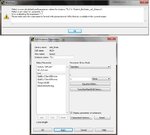
I forgot to say: If I am assigning L=L, - ADS does not accept it
comes following message (see photo below):

- - - Updated - - -

Pin 16 - is temporary (it will be connected to interlayer later), but I am using it now for cross-talk exam...,
About Pins 15/18 : do I need them for electrical connection of separate MLIN to the rest of layout structure in the schematics window?
 

Attachments

  • Warning.jpg
    Warning.jpg
    105 KB · Views: 100

I forgot to say: If I am assigning L=L, - ADS does not accept it
comes following message (see photo below):

Then you made a mistake somewhere - it should work. Maybe you did not define the cell parameter?


About Pins 15/18 : do I need them for electrical connection of separate MLIN to the rest of layout structure in the schematics window?

I was assuming you want to include the layout created by the MLIN in the EM model, i.e. only use the MLIN to "draw" a scalable line. Then of course you don't need these ports. The MLIN will become part of the layout, like other metal polygons.

If you want to simulate the MLIN separately, with the schematic model, that's a different thing. Then you need ports - added manually or configure proper hierarchy for co-simulation so that the MLIN is NOT included in the Momentum model. It all depends what your intended workflow is. Too much details to discuss it by forum or mail, sorry for that.
 

Then you made a mistake somewhere - it should work. Maybe you did not define the cell parameter?

If you want to simulate the MLIN separately...

I will explain shortly:
First I have created a layout (top cond. + ground plain).
Then - created a component and co-simulated its S-parameters in the circuit window.

Now I want to simulate again s-parameters of same layout but changing (sweeping) the size of small part (strip) of it.

I thought that it is possible by cutting and replacing of that small strip by MLIN (of same size).

Is it possible?
 

Yeah, but you didn't get my point: do you want to simulate the MLIN part with the MLIN circuit model (everything EM except MLIN), or re-simulate the whole layout (all EM) with a different size of the MLIN section?

If you want to simulate the MLIN separately, an easy way would be to remove it from the layout, and add it only in the schematic. Then in layout/EM you just need a port where the MLIN is connected to the EM/layout part.
 

...And I will need for simple method only define correct substrate parameters for MLIN..
----------------
Is second way also possible?
("re-simulate the whole layout (all EM) with a different size of the MLIN section")
 

Is second way also possible?
("re-simulate the whole layout (all EM) with a different size of the MLIN section")

Yes, sure, as described above. If the MLIN appears in layout, it can (and usually will) be part of the EM Model.
 

Hello Volker,
I am trying to design everything from the scratch and now i'am getting problems:

1.). I'm creating a component (same as in the photos above) in layout and putting it in to circuit. And adding few ideal components. If i want simulate s-parameters -> comes there a warning that in layout there are 17 pins and in the circuit there are NO pins. It is new for me....
2.). If I am adding 17 pins in the circuit and trying to simulate s-parameters -
comes following new error:
"Error detected by hpeesofsim during netlist flattening.
`I__0' is an instance of an undefined model `LD1_cell_1'. "

Can you please explain what I am doing wrong? May be something with the pins assignment...
 
Last edited:

Status
Not open for further replies.

Part and Inventory Search

Welcome to EDABoard.com

Sponsor

Back
Top