Continue to Site

Welcome to EDAboard.com

Welcome to our site! EDAboard.com is an international Electronics Discussion Forum focused on EDA software, circuits, schematics, books, theory, papers, asic, pld, 8051, DSP, Network, RF, Analog Design, PCB, Service Manuals... and a whole lot more! To participate you need to register. Registration is free. Click here to register now.

RTL Design from timing diagram

Status
Not open for further replies.

hm1622

Junior Member level 1
Joined
Feb 9, 2011
Messages
18
Helped
0
Reputation
0
Reaction score
0
Trophy points
1,281
Location
surat
Visit site
Activity points
1,481
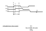
Capture.JPGCapture1.JPG

I dont know from where to start so guys help me with that. i am beginner in RTL design
please help me with RTL(verilog) design of this block.i have some specification
like

• X means a minimum size width for n and p channel transistor width for
the transistors inside the inverter .
• 8X means n and p ch widths are 8 times that of 1X inverter.
• D<9:0> means data lines; these are digital outputs that change after the clock rising edge. Think of it as a digital bus.
 

If you don't know where to start, and you certainly have not explained where you need to finish, how can we possibly give you instructions from start to finish?

D is suppoed to change to wHAT?
 

Your specification seems incomplete.

What is the relation of the outputs to inputs? Do you have to design the inverters first and then use them in your RTL or do you already have the standard cells?

Once you have the complete spec you can start the RTL coding which is followed by synthesis and place & route.
 

A & B = Asynchronous Digital control inputs
X = a minimum size width for n and p channel transistor width for
the transistors inside the inverter.
8X = n and p channel widths are 8 times that of 1X inverter.
D<9:0> = data lines; these are digital outputs that change *after*
the clock rising edge. Think of it as a digital bus.
 

I will try to help but as others have said, your spec is still unclear.

• X means a minimum size width for n and p channel transistor width for
the transistors inside the inverter .
• 8X means n and p ch widths are 8 times that of 1X inverter.
• D<9:0> means data lines; these are digital outputs that change after the clock rising edge. Think of it as a digital bus.

The 1st two points indicate the design of an inverter, for which you need some SPICE tool. You do such exercises typically in the university for very basic CMOS Analog design lab assignments. This has no relation to RTL design.
So I find your statement contradictory - " i am beginner in RTL design please help me with RTL(verilog) design of this block".

I also don't understand any of your attachments. Digital design (RTL) specs are not distributed in this way!

Ask yourself these questions:
What am I trying to achieve?
What are my inputs and what should be the desired outputs, get the proper spec/lab exercise/assignment/handout if you don't have?
Do I need to do an analog design or digital design?
 
  • Like
Reactions: FvM

    FvM

    Points: 2
    Helpful Answer Positive Rating
Status
Not open for further replies.

Part and Inventory Search

Welcome to EDABoard.com

Sponsor

Back
Top