aot
Newbie level 6
Hi,
I am currently building a high power (ideally 100W+ CW) noise blanking gate for the output of an AMT M3205A power amplifier for use in MRI. Basically, even with the blanking circuitry switched in (for all stages in the amplifier) there is a significant amount of noise being emitted from this amplifier, and this is easily seen in the MRI images. The frequency of operation for this is 123.259MHz.
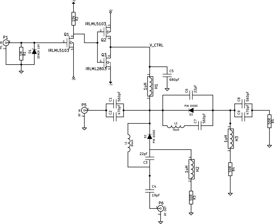
I've got a basic design which is essentially a series/shunt type SPDT switch using PIN diodes, except with parallel resonance circuits around each diode to increase isolation (see schematic at the bottom - this is the basic circuit and the component values change quite a bit, I think the ones in the schematic are what I found simulated well). In QUCS I have built a simulation which works well, but I just can't get good performance for the real thing, especially when driving it with a bit of power. Above about 10W it is reflecting so much back the amplifier goes into overdrive and shuts down!
I built something similar to this for blanking some 1W amplifiers, and got very good results. However the Tx path was in series with a PIN diode forward biased, in this high power version the Tx path is via an inductor in parallel to the reverse biased PIN. It's built as a microstrip layout on FR4, but I've had to jiggle things around and cut the tracks as the board was originally for the 1W version (I don't have access to PCB milling machines here), so there's probably some parasitics there causing a mismatch.
I keep modifying it, but basically the problem I'm having is that the match of the Tx path (via D2) is poor, and this mismatch gets worse with more power from the network analyser.
The former is because of parasitics from the board, D2, C3 etc which means that the Tx path is not purely through C1, C2, L1 and C4, so consequently C4 cannot cancel L1's reactance. I think by working methodically through it all I can figure out the sources, but I'm not sure how to cancel it out. I did build a L matching network on the RF out port (P6) and managed to get the match to 50ohms, but is this the right thing to do?
As for the worse performance with higher powers this could be a few things. My NA might not be calibrated (it's about 15 years old and hasn't seen a service for years), but I recently compared it with some others and found it to perform adequately. There could be some non-linearities in the passive components I am using, but I think this is unlikely as they are decent P90 capacitors from passive-plus (1111P series), and the inductors are hand-wound air-gap, from 1.25mm diameter enamelled copper. The RF chokes aren't fantastic, and have since I've replaced them with parallel resonant traps and get 12k+ from them, which I would have thought would be sufficient.
I think the issue is that the diodes are only reverse biased to 5V, so there's a possibility the Tx power is turning them on, but this would be quite a change that I would need to find a higher voltage dual rail power supply! The PIN's I am using are passive plus PPD1200's (most of my components are non-magnetic types for MRI, this isn't necessary here as the gate isn't going inside the MRI scanner, but I happen to have all the bits already).
I'm a Ph.D student, and my background is Physics, so everything RF is what I have learnt over the past four years, and for the most part that has been building MRI coils and associated low power bits. Also the focus of my project is using that noisy amplifier in the imaging, so I really want to just be able to get this done and move on, but I appreciate that this is probably not a trivial circuit, especially given my limited knowledge, expertise and equipment, and that high power RF is particularly tricky!
Any advice would be particularly useful, I've got some more structured questions below, but general comments would be really appreciated.
1. The matching network I mentioned, is that the right way to sort out the parasitic reactances and get a better match, or should I be series resonating/shunting them out first and then build a matching network if necessary?
2. is this power non-linearity I'm seeing due to the diodes not being reverse biased enough, or is it just due to the design and I should try to account for it when building the matching network.
3. Is this even a good way to build a RF switch, I've had a look on the net and seen some TR switches, many are the series/shunt type T/R switches, perhaps I should be going with those - power handling was my concern though.
Many thanks,
Aaron
 Ωµ
Ωµ
I am currently building a high power (ideally 100W+ CW) noise blanking gate for the output of an AMT M3205A power amplifier for use in MRI. Basically, even with the blanking circuitry switched in (for all stages in the amplifier) there is a significant amount of noise being emitted from this amplifier, and this is easily seen in the MRI images. The frequency of operation for this is 123.259MHz.
I've got a basic design which is essentially a series/shunt type SPDT switch using PIN diodes, except with parallel resonance circuits around each diode to increase isolation (see schematic at the bottom - this is the basic circuit and the component values change quite a bit, I think the ones in the schematic are what I found simulated well). In QUCS I have built a simulation which works well, but I just can't get good performance for the real thing, especially when driving it with a bit of power. Above about 10W it is reflecting so much back the amplifier goes into overdrive and shuts down!
I built something similar to this for blanking some 1W amplifiers, and got very good results. However the Tx path was in series with a PIN diode forward biased, in this high power version the Tx path is via an inductor in parallel to the reverse biased PIN. It's built as a microstrip layout on FR4, but I've had to jiggle things around and cut the tracks as the board was originally for the 1W version (I don't have access to PCB milling machines here), so there's probably some parasitics there causing a mismatch.
I keep modifying it, but basically the problem I'm having is that the match of the Tx path (via D2) is poor, and this mismatch gets worse with more power from the network analyser.
The former is because of parasitics from the board, D2, C3 etc which means that the Tx path is not purely through C1, C2, L1 and C4, so consequently C4 cannot cancel L1's reactance. I think by working methodically through it all I can figure out the sources, but I'm not sure how to cancel it out. I did build a L matching network on the RF out port (P6) and managed to get the match to 50ohms, but is this the right thing to do?
As for the worse performance with higher powers this could be a few things. My NA might not be calibrated (it's about 15 years old and hasn't seen a service for years), but I recently compared it with some others and found it to perform adequately. There could be some non-linearities in the passive components I am using, but I think this is unlikely as they are decent P90 capacitors from passive-plus (1111P series), and the inductors are hand-wound air-gap, from 1.25mm diameter enamelled copper. The RF chokes aren't fantastic, and have since I've replaced them with parallel resonant traps and get 12k+ from them, which I would have thought would be sufficient.
I think the issue is that the diodes are only reverse biased to 5V, so there's a possibility the Tx power is turning them on, but this would be quite a change that I would need to find a higher voltage dual rail power supply! The PIN's I am using are passive plus PPD1200's (most of my components are non-magnetic types for MRI, this isn't necessary here as the gate isn't going inside the MRI scanner, but I happen to have all the bits already).
I'm a Ph.D student, and my background is Physics, so everything RF is what I have learnt over the past four years, and for the most part that has been building MRI coils and associated low power bits. Also the focus of my project is using that noisy amplifier in the imaging, so I really want to just be able to get this done and move on, but I appreciate that this is probably not a trivial circuit, especially given my limited knowledge, expertise and equipment, and that high power RF is particularly tricky!
Any advice would be particularly useful, I've got some more structured questions below, but general comments would be really appreciated.
1. The matching network I mentioned, is that the right way to sort out the parasitic reactances and get a better match, or should I be series resonating/shunting them out first and then build a matching network if necessary?
2. is this power non-linearity I'm seeing due to the diodes not being reverse biased enough, or is it just due to the design and I should try to account for it when building the matching network.
3. Is this even a good way to build a RF switch, I've had a look on the net and seen some TR switches, many are the series/shunt type T/R switches, perhaps I should be going with those - power handling was my concern though.
Many thanks,
Aaron
 Ωµ
Ωµ