Continue to Site

Welcome to EDAboard.com

Welcome to our site! EDAboard.com is an international Electronics Discussion Forum focused on EDA software, circuits, schematics, books, theory, papers, asic, pld, 8051, DSP, Network, RF, Analog Design, PCB, Service Manuals... and a whole lot more! To participate you need to register. Registration is free. Click here to register now.

RF trace jumping and noise test

Zebxcore

Newbie level 6
Joined
Aug 24, 2022
Messages
12
Helped
1
Reputation
2
Reaction score
0
Trophy points
1
Activity points
256
Good day fellas,

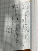
I designed the following board which includes a bias tee, gain amp, and an attenuator which I am still working on since it requires me to program the main IC on an external board to control it via I2C. In the meantime, I would like to make it work and test on it. What I came up with is what you see, a copper strand out from a coaxial cable, of similar width to a 50 ohm trace to short the I/O of the attenuator. At higher frequencies, around 1.5GHz and up, the response is obviously very wavy and bad but I am only concern up to 1GHz. Has anyone a better idea to short it without using copper tape? (I dont have any around).
IMG_9711-min.jpg

Also, with the little testing I have done so far, our signal seems to have added noise to it. I calculated the noise from the LNA (its a HMC636 or HMC589 depending on gain needed) and it seemed to be ok. However, the SNR difference at the RX with and without the amp is astronomical even though the power levels seems good. TX signal is about 18dBm onto a peak antenna with gain of about 2-3dBi over 30-40ft. All this at around 3.4GHz. I know AT&T bought a big portion of the spectrum for low 5G implementation but I am not sure if that could have anything to do with added noise close to 3.5GHz.

Thanks for any help you guys can provide me with :)
 
No, not appropriate. It will disturb Rf Performance. Transmission Lines need Continuity , if you cut the line, there will be a strong reflection at Discontinuity point.
Why don't you pass parallel lines of U3 on Bottom Layer ? Is there any obligation ?
Briefly, do not disturb the RF transmission Lines, find an alternative path for second degree non-RF tracks.
 
Why don't you pass parallel lines of U3 on Bottom Layer ? Is there any obligation ?
Briefly, do not disturb the RF transmission Lines, find an alternative path for second degree non-RF tracks.
TL topology is coplanar with ground, having a continuous ground plane is most important. Attenuator wiring looks acceptable, top wiring of control lines can be found in most reference designs.

At higher frequencies, around 1.5GHz and up, the response is obviously very wavy and bad but I am only concern up to 1GHz. Has anyone a better idea to short it without using copper tape? (I dont have any around).
Are you reporting real or expected measuring results?

I won't expect much effect of the mismatched jumper wire, may be 0.5 dB drop at higher frequencies. Comparable to the effect of Coilcraft bias chokes. Although it seems easy to use e.g. a bundle of thin wires to better match trace impedance.

Also, with the little testing I have done so far, our signal seems to have added noise to it. I calculated the noise from the LNA (its a HMC636 or HMC589 depending on gain needed) and it seemed to be ok. However, the SNR difference at the RX with and without the amp is astronomical even though the power levels seems good. TX signal is about 18dBm onto a peak antenna with gain of about 2-3dBi over 30-40ft. All this at around 3.4GHz. I know AT&T bought a big portion of the spectrum for low 5G implementation but I am not sure if that could have anything to do with added noise close to 3.5GHz.
Did you also measure amplifier noise with just 50 ohm input termination? The input bias circuit suggests that you are using an active antenna or external amplifier.
 
The mismatch from the wire impedance (which is about 37 ohms, assuming the SMD passive components are 0603), wouldn't be a big issue.
But crossing the digital lines of U3 directly under the wire, would be a problem catching the noise.
One option would be to use a thin semirigid coax cable to cross over those lines.
 
No, not appropriate. It will disturb Rf Performance. Transmission Lines need Continuity , if you cut the line, there will be a strong reflection at Discontinuity point.
Why don't you pass parallel lines of U3 on Bottom Layer ? Is there any obligation ?
Briefly, do not disturb the RF transmission Lines, find an alternative path for second degree non-RF tracks.
Thanks for the reply. I understand this but the footprint is covered by some tape rather than being below the impedance controlled trace. I attach a more detailed view of the final board for clarity. My concern is the mismatch the copper piece will have rather than having a 50 ohm trace at lower frequencies and if at this length, exactly 450mil, it will act as a radiating element on the 3-4GHz band.
IMG_9760-min.jpg

I won't expect much effect of the mismatched jumper wire, may be 0.5 dB drop at higher frequencies. Comparable to the effect of Coilcraft bias chokes. Although it seems easy to use e.g. a bundle of thin wires to better match trace impedance.


Did you also measure amplifier noise with just 50 ohm input termination? The input bias circuit suggests that you are using an active antenna or external amplifier.
We don't have much equipment so I could only do a one path 2-port calibration on our VNA and tested S21 and S11, flipped the DUT and tested S12 and S22. However, I don't know if doing this equates to a full 2-port calibration and test. Below are the results using a GALI3+. At 1.5GHz or so, S21 starts to come down. (Sorry for the pics, both screens are CRT)

S21.jpg
S11.jpg
S12.jpg
S22.jpg

We have a Spectrum analyzer, Agilent 8562A, I have been playing around with to figure out noise figures on most amps we have using the Gain method since I don't have a calibrated noise source nor a signal generator to do the Y-Factor method nor any other method to be frank. I just cant find a good video or explanation on how to properly set up RBW and VBW on this specific piece of equipment as well as using the noise marker, but I am trying my best to figure this part out. For now, my main concern is figuring out why once I implement this device in our system, our receiver just go nuts and our SDR is very tight (Cannot attenuate more than 20dBm down or signal is lost while not using this amp we get about -50dBm before we see the signal come down). My guess was the amp, but I have tried about 5-6 different kinds. From the ones mentioned, to GALI3+, GALI6+, PHA-1+. A quick block diagram of my test setup is included for reference.

Thanks again guys!
IMG_9761-min.jpg
 

Attachments

  • IMG_9761-min.jpg
    IMG_9761-min.jpg
    807.7 KB · Views: 41

LaTeX Commands Quick-Menu:

Similar threads

Part and Inventory Search

Welcome to EDABoard.com

Sponsor

Back
Top