Continue to Site

Welcome to EDAboard.com

Welcome to our site! EDAboard.com is an international Electronics Discussion Forum focused on EDA software, circuits, schematics, books, theory, papers, asic, pld, 8051, DSP, Network, RF, Analog Design, PCB, Service Manuals... and a whole lot more! To participate you need to register. Registration is free. Click here to register now.

rf connector to fit substrate thickness question

yefj

Advanced Member level 4
Joined
Sep 12, 2019
Messages
1,196
Helped
1
Reputation
2
Reaction score
3
Trophy points
38
Activity points
7,223
Hello, my substrate is FR4 1.6mm and signal thickness is 1oZ (0.035mm)
the width of a trace is about 0.2mm also there will be copper pour around the trace with 0.2 spacing from the trace
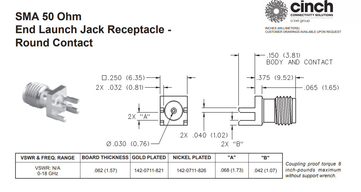
I have found connector shown in the link below.
but i am not sure if would be able to solder this connector to the PCB.
from the data sheet bellow they say that the distance between pins is 2'A'
A=1.73mm which is 2*1.72 much higher then 1.6mm.

How do i find a connector which could fit my 1.6mm and trace 1oZ thichness?
they is no such category in digikey filter,so how could i know is this connector whould fit my PCB?
Thanks
1695633228290.png
 
The top layer dimensions share the same width on the recommended layout as the connector.
Why are you confused?

Your "bottom" layer should be a ground plane, as described in your link. FIX THAT!

The tabulated dimensions "A", "B", "C", "D", and "E" were determined experimentally to achieve low VSWR (typically less than 1.5 up to 18GHz). The circuit board used for these tests was double-sided FR 4 with 1 oz. copper on both sides. The copper was left on the bottom of the board to create a ground plane for the 50 Ohm microstrip structure.
Now you are wondering why is the FR4 gap smaller than the SMA air gap from center pin to gnd.=.
Compare the cross-section thickness of 1 oz Cu to the connector pins. Since Zo^2=L/C and the length is shared and C is a function of area/gap ratio * εr.

Can you estimate or compute why the gaps are different with wider pads extended only on the inside?
1695760811978.png


1695760775294.png


Adding more center soldering will lower the impedance slightly.

Regarding your incorrect concern on thickness, it is 1.73 mm in 2x locations vs 1.6 mm PCB so 0.1mm can easily be gap filled with solder on the ground plane contact areas.
 
Last edited:

LaTeX Commands Quick-Menu:

Similar threads

Part and Inventory Search

Welcome to EDABoard.com

Sponsor

Back
Top