Continue to Site

Welcome to EDAboard.com

Welcome to our site! EDAboard.com is an international Electronics Discussion Forum focused on EDA software, circuits, schematics, books, theory, papers, asic, pld, 8051, DSP, Network, RF, Analog Design, PCB, Service Manuals... and a whole lot more! To participate you need to register. Registration is free. Click here to register now.

Resistance between PCB trace and GND plane

Status
Not open for further replies.

hioyo

Advanced Member level 4
Joined
Aug 18, 2021
Messages
116
Helped
0
Reputation
0
Reaction score
2
Trophy points
18
Activity points
899
Dear Team,

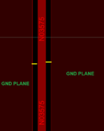
I don't know this is a nonsense question or not.
Please see the below image.
You can see the trace which is red in color and it is surrounded by a GND plane.
The clearance is shown with Yellow lines and it is.12mm.

My question is what is the resistance existing in the region of clearance(Shown with blue lines)

1644839088699.png


Regards
HARI
 

Attachments

  • 1644838885852.png
    1644838885852.png
    7 KB · Views: 145

Negligible for many, but possibly not for all purposes. Volume and surface resistance values for PCB substrates are given in datasheets with large margin between typical and guaranteed values. You can calculate after you have defined the test geometry completely, which istn't done in your picture (no test structure length, no substrate thickness, no specification of bottom side).

You should also consider that the actual resistance depends strongly on surface contamination, relative humidity and water absorbed by the PCB. A typical situation to get unsuficient resistance is surface condensation.
 

Hi,

If you are concerened about leakage current, then read about "guarding of signals".

Klaus
 
Please also note that the clearance you provided is not enough to calculate resistance becasue it depends on the length of the trace as well.
 

Thank you....
I want that resistance to be in Tera Ohms.
This resistance is high enough to be considered negligible for practical purposes.
--- Updated ---

T
Hi,

If you are concerened about leakage current, then read about "guarding of signals".
Thank you...
I am not in a situation to provide guard rings.
I need to do guarding by using keep out area.
But I don't know how to keep out area I need to provide.
The resistance required shoud be in Tera Ohms
--- Updated ---

Negligible for many, but possibly not for all purposes. Volume and surface resistance values for PCB substrates are given in datasheets with large margin between typical and guaranteed values. You can calculate after you have defined the test geometry completely, which istn't done in your picture (no test structure length, no substrate thickness, no specification of bottom side).

You should also consider that the actual resistance depends strongly on surface contamination, relative humidity and water absorbed by the PCB. A typical situation to get unsuficient resistance is surface condensation.
Thank you very much.
May I know how to calculate the resistance(As Shown in Blue) if I know the test structure length,thickness, and spec of the bottom side.
My bottom side a GND plane
 
Last edited:

Status
Not open for further replies.

Part and Inventory Search

Welcome to EDABoard.com

Sponsor

Back
Top