Continue to Site

Welcome to EDAboard.com

Welcome to our site! EDAboard.com is an international Electronics Discussion Forum focused on EDA software, circuits, schematics, books, theory, papers, asic, pld, 8051, DSP, Network, RF, Analog Design, PCB, Service Manuals... and a whole lot more! To participate you need to register. Registration is free. Click here to register now.

Reduce ringing using EMI filter block

Status
Not open for further replies.
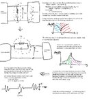
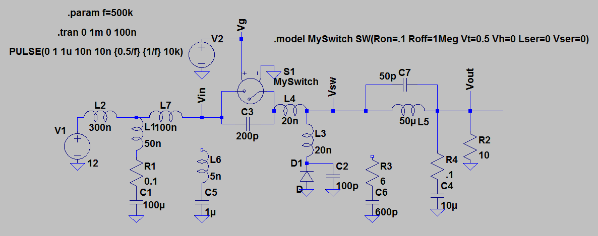
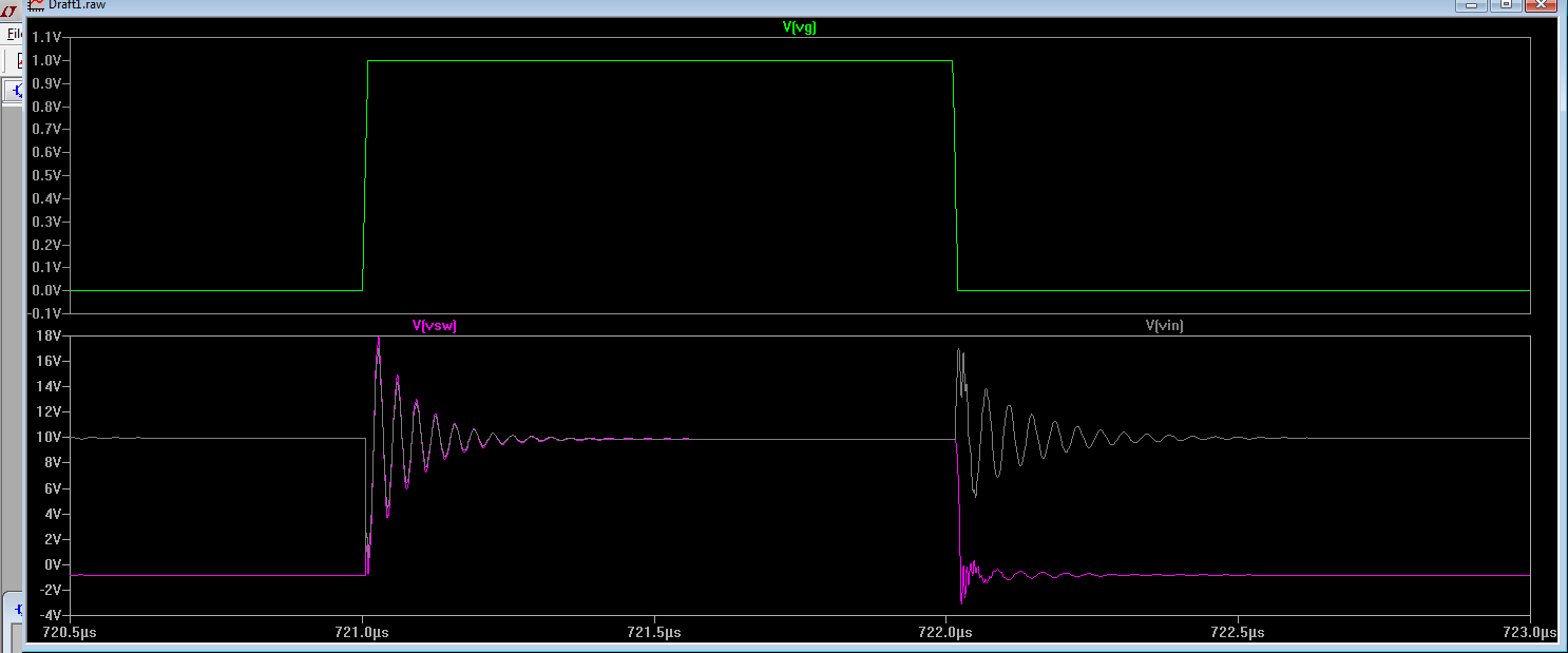
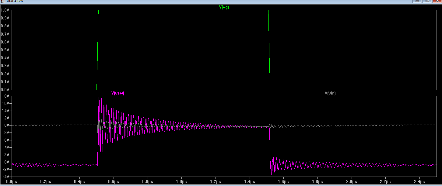
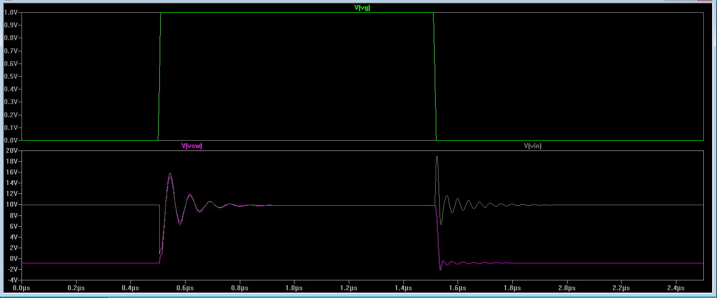
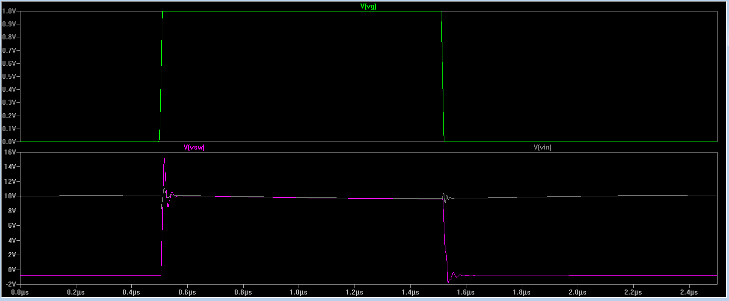
The most important point is to understand, that switching frequency voltage differences along ground wires and PCB ground traces are real.

They show up as measurement artefacts but also affect the circuit operation in general. There are different ways to get reliable measurements under this conditions. Using differential probes is one of them, different usage of conventional probes, e.g. with bajonet ground tips, another one. Be aware of the problem and try to distinguish between real signals and artefacts as far as possible.
 

Hello guys,

I would like to have some additional discussion. My arguments are in the newly attached.

Do you think a series LC tank circuit worth trying to suppress noise riding on my +28V DC?
 

Attachments

  • series filter.jpg
    series filter.jpg
    334.1 KB · Views: 56

Again, I'm not saying you should just do one instead of the other. They're both effective in different ways.
Here's a schematic showing most of the possible parasitic resonances in the circuit:


Notice that C5+L6 (the high frequency ceramic capacitor) and R3+C6 (the RC snubber network) is unattached for now. Here's what the transient waveforms at the switch "drain" and "source look" like, as is:


Now we attach the input bypass cap C5+L6, and we get this:

Things actually look a lot worse. This isn't too surprising. We've decreased the impedance at the source quite a bit, but not this has caused other resonances to become less damped and higher frequency.

Now we disconnect C5+L6, and then attach the snubber:


And now lets try using both the input bypass cap and the snubber:


So we can see that when we have lots of parasitics in the circuit, neither the input bypassing or the RC snubber do a great job on their own. Using them both together provides the best results.

Hi mtwieg, could you share your above LTspice schematic if you still have it? I would like to add more simulations using the layout you've done out.
 

Status
Not open for further replies.

Similar threads

Part and Inventory Search

Welcome to EDABoard.com

Sponsor

Back
Top