Continue to Site

Welcome to EDAboard.com

Welcome to our site! EDAboard.com is an international Electronics Discussion Forum focused on EDA software, circuits, schematics, books, theory, papers, asic, pld, 8051, DSP, Network, RF, Analog Design, PCB, Service Manuals... and a whole lot more! To participate you need to register. Registration is free. Click here to register now.

Reduce ringing using EMI filter block

Status
Not open for further replies.
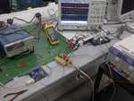
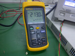
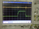
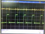
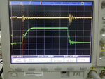
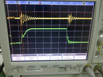
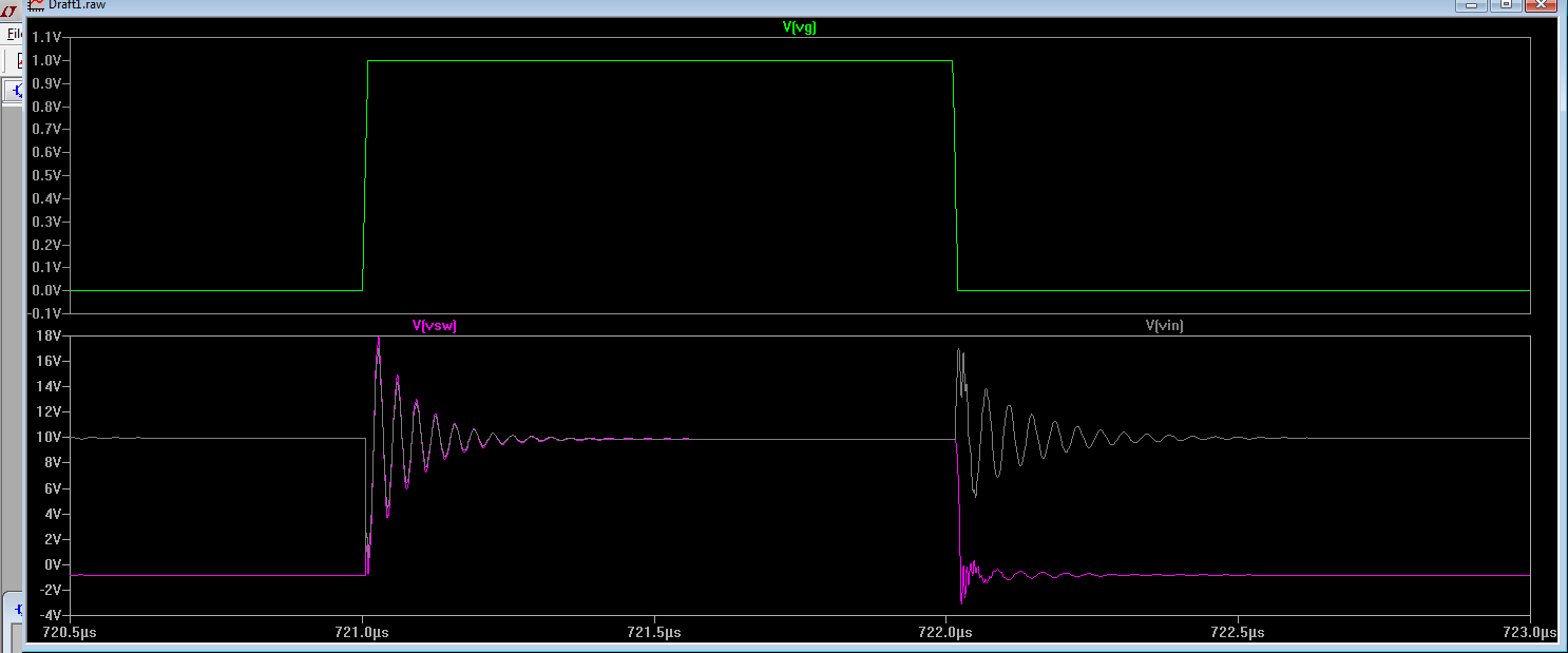
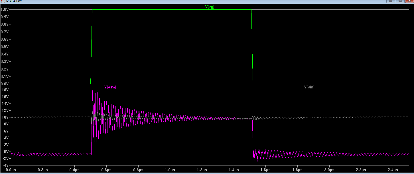
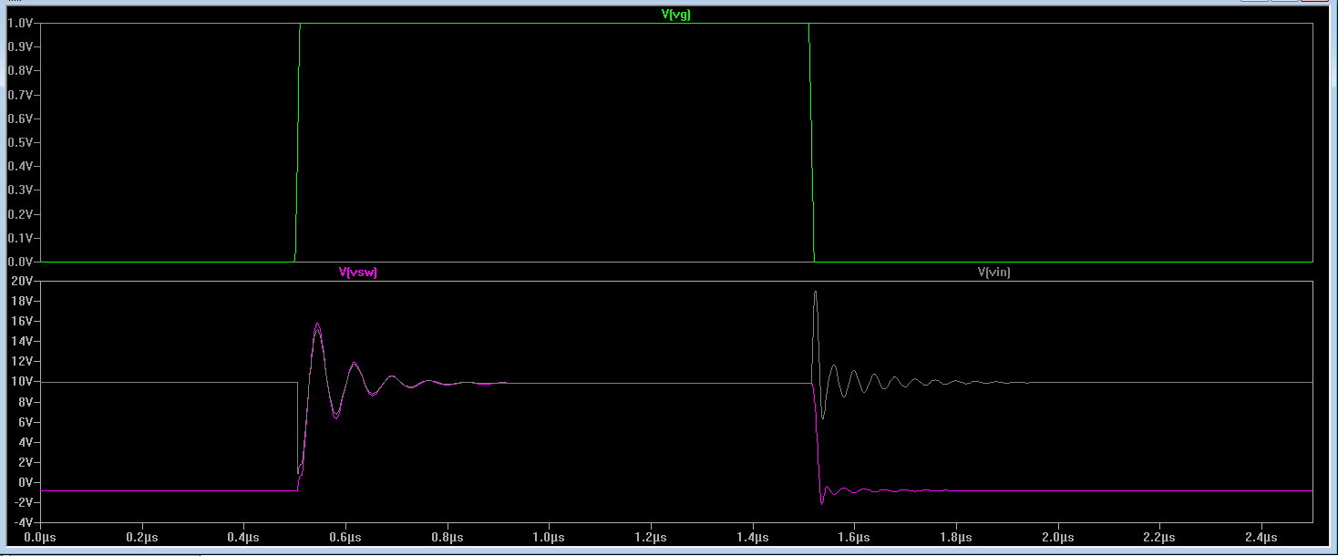
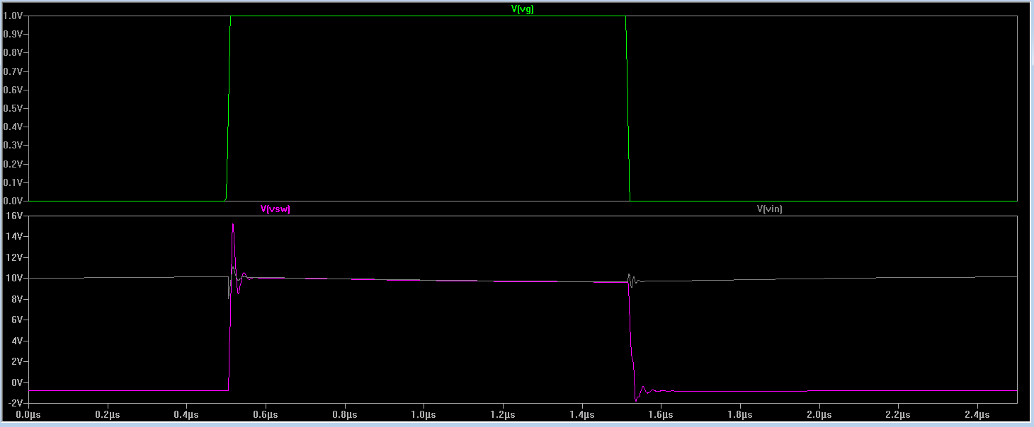
Rgate is very high now according to the waveform. A trade-off between oscillations and losses seems necessary.

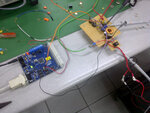
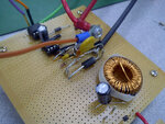
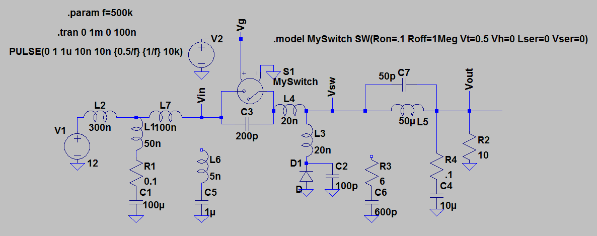
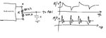
I would build the circuit on a RF stripboard with a continuous copper plane on the top side (with voids around the drilled holes) and add low impedance bypass capacitors for in- and outputs.
 

Hi,

I'm reporting live from my laboratory. I just made another discovery.

All along I've been using AC coupling to moniter the vout noise amplitude.

when I forgot to connect the probe to the output.

Therer is also about the same noise waveform occurring, the only difference is
the amplitude! (still about 1.2V pk-pk).

Something is wrong here right? What conclusion could we draw?

The noise is radiated instead of conducted? Or it is still radiated because one set of
probes' GND is touching the PSG, the other is touching CG,

So cross talk occurs within the o-scope?
 

Blue waveform - Vs w.r.t. Power GND(PSG)
Green waveform - V(gs)
Yellow waveform - V(out) w.r.t CG (or output filter's GND)

2.jpg shows w/o RC snubber:
Noise pk-pk is about 3.5V (Bad!)

3.jpg shows RC snubber connected across V(s) and PSG with R= 8ohms, C = 820pF:

1.jpg is when I increase Rgate slowly using a potentiometer:

This method seems to be the best for attenuating output voltage noise to about only 1V pk-pk!
But the consequence is high, it causes my nMOS to heat about mor than 160 degrees celcius!

I intend to use heat sink to cool the MOSFET out.

Besides this? I've tried bypassing V(d) w.r.t. PSG but all are rather useless.

Have also known that increasing RC snubber would somehow damp the rising edge at V(s) w.r.t PSG, but there is a limit I can go. Basically 820pF seems the best.

I've also seperate AGND with PSG so that both GNDs are only connected to each other through the muRata filter.

Really at wits end to suppress this noise. Attached is the bigger view of my table. Hope can receive more suggestion.
Okay it sounds like you've just been trying to solve the problem by taking shots in the dark without much understanding of how things like RC snubbers and gate resistors actually work. You should remove the gate resistor and the "snubber" you added and start from scratch.

Here's a couple tips:
1. RC snubbers need to be pretty accurately sized. Simply throwing some random values there usually won't help at all. You need to follow an actual procedure for getting the right damping factor at the right frequency. Here's a decent guide from national: **broken link removed**
2. Notice that this procedure assumes that your ringing is mainly one frequency. That doesn't seem to be the case with you; your ringing is comprised of many tones overlapping, meaning you have several parasitic LC combinations working together. These can be due to:
  • Switching node capacitance resonating with diode inductance (this is the most common cause)
  • Switching node capacitance resonating with the FET inductance
  • Self resonance of the input bypass capacitor
  • Self resonance of the inductor (this is rarely the issue)
If you have many sources of ringing, then it's pretty much impossible to dampen them all. You need a better layout to suppress some of them. You need an excellent high frequency input bypass capacitor (a good ceramic or film cap, a few uF in value) connected right between the FET drain and the diode anode. If your ringing is still "polyphonic" then you need to reduce the parasitic inductance around that high frequency loop formed by the input bypass cap, the FET, and the diode. Just shrink the loop area as much as possible. Once the ringing is reduced to a single tone you can apply an RC snubber with the described procedure. As FvM implies, reducing the impedance of that high frequency loop is the absolute best way to address ringing. A snubber is an inferior way to reduce ringing, but is often necessary because sometimes it's not possible to get things working without it.
3. Your gate resistor is obviously too high now. The purpose of the gate resistor is to simply damped any ringing on the gate waveform. Usually something in the range of 1-10 ohms is sufficient.
4. As you've noticed, scope measurements aren't always trustworthy. Some EMI will be radiated, some will be conducted. Often it's very difficult to tell the two apart. But if your layout is good and you apply proper snubbing, both will be greatly attenuated. But not completely. That's simply the way hard switched converter are.
 
Mtwieg, foremost thanks for your detailed explanation.

1. RC snubbers need to be pretty accurately sized. Simply throwing some random values there usually won't help at all. You need to follow an actual procedure for getting the right damping factor at the right frequency. Here's a decent guide from national: **broken link removed**

My first approach in obtaining the RC value is actually also based on this link you've provided, however I am not sure if I've done it wrongly because instead of randomly inserting a cap across the switch node and the FW diode anode until I hit twice the period of the initial ringing period as indicated by the guide you appended, I've followed: http://www.aosmd.com/res/application_notes/power-ics/PIC-005.pdf. In the latter, it uses the dominating capacitance, which is believed to be the capacitance of the FW diode in this case and x3 to get the Csnub. It then uses R=2*pi*f(ring)*Lp where Lp can be calculated using another formula as written in the guide. Which method is better?

2. Notice that this procedure assumes that your ringing is mainly one frequency. That doesn't seem to be the case with you; your ringing is comprised of many tones overlapping, meaning you have several parasitic LC combinations working together. These can be due to:
  • Switching node capacitance resonating with diode inductance (this is the most common cause)
  • Switching node capacitance resonating with the FET inductance
  • Self resonance of the input bypass capacitor
  • Self resonance of the inductor (this is rarely the issue)
If you have many sources of ringing, then it's pretty much impossible to dampen them all. You need a better layout to suppress some of them. You need an excellent high frequency input bypass capacitor (a good ceramic or film cap, a few uF in value) connected right between the FET drain and the diode anode.

Again, if I am using any "few uF" capacitance to do trial and errors, I would be shooting in the dark once more. How should I calculate this C value? By using Z=1/(2*pi*f*C), if yes, the f is the freq of the ring? and Z=?

If your ringing is still "polyphonic" then you need to reduce the parasitic inductance around that high frequency loop formed by the input bypass cap, the FET, and the diode. Just shrink the loop area as much as possible.

From this guide (**broken link removed**), it says the input bypass cap should be preferably installed as near as possible to the Drain and the lead of the rectifier. Is this the same as what you meant as above?

Once the ringing is reduced to a single tone you can apply an RC snubber with the described procedure. As FvM implies, reducing the impedance of that high frequency loop is the absolute best way to address ringing.

Ok, I've heard many has said about impedance here and there, from what I know, impedance is really like a resistance but varies with freq. (ZL = 2*pi*f*L and Zc = 1/2*pi*f*C). So if we reduce impedance, how could we filter out ringings?

I think the way I try to connect the understanding of bypassing with impedance is relatively weak. I hope you can perhaps explain a little more perhaps with some simple examples which you think is easy for my level.
 

Something is wrong here right? What conclusion could we draw?

The noise is radiated instead of conducted? Or it is still radiated because one set of
probes' GND is touching the PSG, the other is touching CG,

So cross talk occurs within the o-scope?

I guess you still connected the probe ground? in the frequency range below 100 MHz, we can still mostly conducted interferences in the vicinity.
 

I guess you still connected the probe ground? in the frequency range below 100 MHz, we can still mostly conducted interferences in the vicinity.

Yes, I am still using the probe ground with no other choice. Basically there are 2 operationg channels in my o-scope. One is the typical hook + crocodile clip kind of probe, the other channel is from a differential probe measurements.

Attached is how I connect the probes, and what type of diff probes Im using, besides being messy a little, do you've anything to point out?
 

Attachments

  • a.jpg
    a.jpg
    121.7 KB · Views: 62
  • b.jpg
    b.jpg
    147 KB · Views: 60
  • c.jpg
    c.jpg
    147.8 KB · Views: 63
  • d.jpg
    d.jpg
    117.5 KB · Views: 66

The photos shows the various ways how switching frequency inteferences can be injected in the measurement path.

For more significant measurements, straight ground connections to the probe ground ring, e.g. using bajonet tips or connectors soldered to the circuit are preferable. In addition, each probe cable should be equipped with a large toroid core as common mode filter, giving room for multiple windings.
 

Hi guys,

As advised, I've removed the 100uF Electrolytic cap and replaced it with a 10nF ceramic cap (that's because this is the biggest ceramic cap I've at the moment, my orders are coming in tomorrow).

Delighted, I've seen a tremedous attenuation of noise pk-pk signal to about a good 1V pk-pk! (see attached)

But the drawback seems to be that the nMOS gets heated up to about 200+ degrees celcius!(see attached) Could it be, because there is no R in series with my +Vin bypass cap and therefore the heat got dissipated in the mosfet through its intrinsic resistance instead?

Next observation made is there also seems a little trade off now at the noise occurring at the falling edge of V(gs).

My guess would be I need to add another capacitor across drain-source to suppress this turn-off transient?

I am so eager to get that overall suppression to a target of <0.8V (mainly 3% ripple).

EDIT: I know the loop from the input bypass cap, FET, schottky diode seems a little too big or long now, thats because because i need to solder the pin quick slot-in so that I could change the capacitance value conveniently. Once the value is finalised, I'll solder it firmly on the stripboard to reduce the loop area.
 

Attachments

  • 4.jpg
    4.jpg
    106.2 KB · Views: 62
  • 1.jpg
    1.jpg
    100.5 KB · Views: 54
  • 2.jpg
    2.jpg
    118.3 KB · Views: 56
  • 3.jpg
    3.jpg
    134.2 KB · Views: 57
Last edited:

As advised, I've removed the 100uF Electrolytic cap and replaced it with a 10nF ceramic cap (that's because this is the biggest ceramic cap I've at the moment, my orders are coming in tomorrow).
It would be interesting to see the input waveform in this situation.

You are effectively shifting input bypassing to the power supply this way and spilling the pulsed input current around. Due to the wire inductance, the edges are slower and less output transients generated. But there's no alternative to input bypass capacitors with sufficient energy storage capability and low series inductance + resistance.
 
My first approach in obtaining the RC value is actually also based on this link you've provided, however I am not sure if I've done it wrongly because instead of randomly inserting a cap across the switch node and the FW diode anode until I hit twice the period of the initial ringing period as indicated by the guide you appended, I've followed: http://www.aosmd.com/res/application_notes/power-ics/PIC-005.pdf. In the latter, it uses the dominating capacitance, which is believed to be the capacitance of the FW diode in this case and x3 to get the Csnub. It then uses R=2*pi*f(ring)*Lp where Lp can be calculated using another formula as written in the guide. Which method is better?
The method you linked seems equivalent to mine, but I emphasize that this method should be done experimentally. You'll never really know what the parasitic node capacitance or inductance is beforehand. Your link glosses over how to actually determine those parameters, while my link gives a method for experimentally doing so. But as I said, applying that method isn't really possible unless your ringing is monophonic.
Again, if I am using any "few uF" capacitance to do trial and errors, I would be shooting in the dark once more. How should I calculate this C value? By using Z=1/(2*pi*f*C), if yes, the f is the freq of the ring? and Z=?
Heh, point taken. This is a case where rigorous calculations aren't necessary. What you want the capacitor to do is provide the lowest impedance possible for the input switching currents. You want its inductance to be negligible (like 10nH max), and its capacitance probably isn't major. Just go for some value between 100nF and 10uF for now. It's more about inductance than capacitance.

From this guide (**broken link removed**), it says the input bypass cap should be preferably installed as near as possible to the Drain and the lead of the rectifier. Is this the same as what you meant as above?
Yes.

Ok, I've heard many has said about impedance here and there, from what I know, impedance is really like a resistance but varies with freq. (ZL = 2*pi*f*L and Zc = 1/2*pi*f*C). So if we reduce impedance, how could we filter out ringings?
The parasitic components of the SMPS itself form filters with various resonances. If we apply hard switching transients to nodes of the filter (as is always the case with a buck converter) we will excite those resonances and get horrible ringing. We can address this by adding more filtering components to the output of the filter, but this is usually not a preferable (or effective) strategy. So rather we actually try to manipulate the existing "filter" by increasing the resonant frequencies (by reducing parasitic inductances) or by dampening them (by adding dissipative snubbers).

---------- Post added at 08:23 ---------- Previous post was at 08:07 ----------

Hi guys,

As advised, I've removed the 100uF Electrolytic cap and replaced it with a 10nF ceramic cap (that's because this is the biggest ceramic cap I've at the moment, my orders are coming in tomorrow).
Hey, we never said to remove that! Having a large capacitor on the input is important for filtering at low frequencies. Generally you have a few different input capacitors which together function across a broad frequency range.
But the drawback seems to be that the nMOS gets heated up to about 200+ degrees celcius!(see attached) Could it be, because there is no R in series with my +Vin bypass cap and therefore the heat got dissipated in the mosfet through its intrinsic resistance instead?
First of all I kind of have to doubt your measurement... FETs can't survive those temperatures, and if that were the case I'd expect to see the insulation melting off your wires...

But anyways, I can't see any good reason why replacing the input capacitor should cause excess heating... hard to tell without seeing the switching node waveforms, or some current waveforms. Are these tests done with a load on the output?
Next observation made is there also seems a little trade off now at the noise occurring at the falling edge of V(gs).
It should be expected that the ringing is stronger during switch turn off, because the current at that time is greater than at turn on. This is especially true when operating in DCM (in which case there should be very little ringing on turn on, since the current is zero).
My guess would be I need to add another capacitor across drain-source to suppress this turn-off transient?
No, simply adding a capacitor to that node is a very poor solution. It may dampen the ringing a bit, but it will hurt your efficiency significantly. You want to apply a RC snubber there (assuming you've reduced your ringing to one frequency).
 
Hey, we never said to remove that! Having a large capacitor on the input is important for filtering at low frequencies. Generally you have a few different input capacitors which together function across a broad frequency range.

Alright, I've no problem understanding that putting multiple bypass cap in parallel would:

1) effectively decrease R(equivalent) because of 1/Req = 1/R1+1/R2+...+1/Rn

2) decrease inductance as well cause just like resistor, they add up in series while reduces when in parallel

3) capacitance works the opposite with inductance, as they add up in parallel and reduces while in series

Ok point no. 3 is abit shady because assuming I've a 100uF retained as my +Vin input bypass cap, adding, say a 100nF across as my second input bypass will yield an equivalent Ceq = 100uF + 100nF = 100.1uF. Which is an 0.1% increment if you like.

So the question is how do this specific configuration allows to attenuate both lower freq and higher freq "noise" when in the first case, we have 100uF, second case 100.1uF. Not much difference.

Could it be due to superposition, for high freq components, it gets absorbed by the 100nF ceramic, and the energy "noise" with lower freq, gets absorbed by the bigger cap? Is this argument right? If yes, the most ideal case is to have many many many capacitors (eg: 100uF, 10uF, 1uF, 0.1uF, 0.01uF ..... etc) all connected as my input bypass? Or rather we find out the participating noise's freq and select our different bypass cap values accordingly?


First of all I kind of have to doubt your measurement... FETs can't survive those temperatures, and if that were the case I'd expect to see the insulation melting off your wires...

But anyways, I can't see any good reason why replacing the input capacitor should cause excess heating... hard to tell without seeing the switching node waveforms, or some current waveforms. Are these tests done with a load on the output?

Yes, all tests were done with the output connecting to an electronic load which is set to constant Current (CC) mode, drawing a CC of 3.5714A.

It might eventually melt if I allowed to let it run for one or two more mins. I think there is no melting occurring mainly because I had immediately switched off the system once it hit the 200 degrees celcius high!

Also, as you can see in 3.jpg (in #28 post), or a zoomed version in b.jpg (in #26 post), there are two ring terminals secured to the TO-220 drain mounting tab. One is the +Vin 100V (with red insulating jacket), the other is basically an thermal couple being clamped with a blue ring terminal so that I could firmly secured together with the MOSFET.

You want to apply a RC snubber there (assuming you've reduced your ringing to one frequency).

I believe your "there" is referring to the nMOS's source and the anode of the FW diode? Or do you meant the drain and source of the MOSFET?
 

Alright, I've no problem understanding that putting multiple bypass cap in parallel would:

1) effectively decrease R(equivalent) because of 1/Req = 1/R1+1/R2+...+1/Rn

2) decrease inductance as well cause just like resistor, they add up in series while reduces when in parallel

3) capacitance works the opposite with inductance, as they add up in parallel and reduces while in series

Ok point no. 3 is abit shady because assuming I've a 100uF retained as my +Vin input bypass cap, adding, say a 100nF across as my second input bypass will yield an equivalent Ceq = 100uF + 100nF = 100.1uF. Which is an 0.1% increment if you like.

So the question is how do this specific configuration allows to attenuate both lower freq and higher freq "noise" when in the first case, we have 100uF, second case 100.1uF. Not much difference.
This analysis works when the capacitors are ideal. They're not ideal in real life, which is why we do these things. All capacitors have ESL (effective series inductance) and ESR (effective series resistance). This leads to them having a self resonant frequency, above which their impedance will look like an inductor (and will increase linearly with frequency). Many electrolytic capacitors have large ESL, making them ineffective for bypassing high frequency signals. Small surface mount ceramic capacitors have much lower ESL, and thus will perform well at higher frequency. I can guarantee that at 20MHz, a tiny surface mount 10nF capacitor will have a lower impedance than a big axial 100uF electrolytic, simply due to the fact that the electrolytic will have a higher ESL. The lead length of the capacitor, along with and PCB traces or other wiring adds to the ESL.
Could it be due to superposition, for high freq components, it gets absorbed by the 100nF ceramic, and the energy "noise" with lower freq, gets absorbed by the bigger cap? Is this argument right?
Yes, basically. A given bypass capacitor will often have a limited frequency range over which is effective. So for very large bandwidth circuits (like SMPS) you'll need a few different capacitor types to cover the full range.
If yes, the most ideal case is to have many many many capacitors (eg: 100uF, 10uF, 1uF, 0.1uF, 0.01uF ..... etc) all connected as my input bypass? Or rather we find out the participating noise's freq and select our different bypass cap values accordingly?
It depends on the application. In general you can usually get away with just two capacitor types (like electrolytic + ceramic). With RF circuits you sometimes need more, but for you, two types should be enough.

Some engineers will actually match up the self resonant frequency of electrolytic capacitors to the switching frequency of a power supply in order to get very low ripple without needing fancy high frequency capacitors at all. I don't recommend trying that though. That certainly won't work for the kind of "noise" you're seeing, which is caused by undamped ringing, not ripple current.


Yes, all tests were done with the output connecting to an electronic load which is set to constant Current (CC) mode, drawing a CC of 3.5714A.
Does it still get hot if the load is decreased significantly, or is removed entirely?
It might eventually melt if I allowed to let it run for one or two more mins. I think there is no melting occurring mainly because I had immediately switched off the system once it hit the 200 degrees celcius high!
If the FET is still functional after that, then I have to believe that the measurement is wrong. There's really no way a FET can reach those temperatures without being destroyed (unless it's a SiC device).

I believe your "there" is referring to the nMOS's source and the anode of the FW diode? Or do you meant the drain and source of the MOSFET?
The source of the N FET and the cathode of the flywheel diode, yes.
 

Hi Mtwieg,

Linking back to one of the guides I've found (see:**broken link removed**), I've tried to find an adequate explanation why suppressing noise at output due to turn-on transient could be more effective by adding a small but high freq effective ceramic bypass @ +Vin, rather than a RC snubber across the FW diode.

My thoughts are, because during turn-on, nMOS is switched on, the +Vin is effectively connected to the switch node, so coupling +Vin is like coupling the switch node.

During turn-off, SW disconnected, so only a RC across the FW diode would really be the last effective resort in suppressing noise occurred due to turning off.

I understand you've mentioned about the various resonant possibilities among different components, but could really only spot out 2 resonating loop, 1) turn on: +Vin, FET, main L, output C, 2) turn-off: schottky (or FW) diode, main L, output C

Is my concept "quite" right?

EDIT: I've just "proven" experimentally that removing and inserting the 100nF parallel input +Vin bypass cap really affects only the output noise occurred at the rising edge without affecting or attenuating (basically has no effect) for the output noise during falling edge. The attached shows the two different test situations:

From without.jpg (100nF +Vin ceramic bypass not added): we see that the output transient at turn-on has a higher 2V pk-pk.

From with.jpg (100nF +Vin ceramic bypass added): we see that the same noise being suppressed to an incredible 1.05V pk-pk!

But observations from two waveform graphs shows no effect in attenuating nosie at occurred during at falling-edge!
 

Attachments

  • with.jpg
    with.jpg
    120.3 KB · Views: 53
  • without.jpg
    without.jpg
    127.5 KB · Views: 48
Last edited:

Hi Mtwieg,

Linking back to one of the guides I've found (see:**broken link removed**), I've tried to find an adequate explanation why suppressing noise at output due to turn-on transient could be more effective by adding a small but high freq effective ceramic bypass @ +Vin, rather than a RC snubber across the FW diode.
Again, I'm not saying you should just do one instead of the other. They're both effective in different ways.
My thoughts are, because during turn-on, nMOS is switched on, the +Vin is effectively connected to the switch node, so coupling +Vin is like coupling the switch node.

During turn-off, SW disconnected, so only a RC across the FW diode would really be the last effective resort in suppressing noise occurred due to turning off.

I understand you've mentioned about the various resonant possibilities among different components, but could really only spot out 2 resonating loop, 1) turn on: +Vin, FET, main L, output C, 2) turn-off: schottky (or FW) diode, main L, output C

Is my concept "quite" right?
Here's a schematic showing most of the possible parasitic resonances in the circuit:


Notice that C5+L6 (the high frequency ceramic capacitor) and R3+C6 (the RC snubber network) is unattached for now. Here's what the transient waveforms at the switch "drain" and "source look" like, as is:


Now we attach the input bypass cap C5+L6, and we get this:

Things actually look a lot worse. This isn't too surprising. We've decreased the impedance at the source quite a bit, but not this has caused other resonances to become less damped and higher frequency.

Now we disconnect C5+L6, and then attach the snubber:


And now lets try using both the input bypass cap and the snubber:


So we can see that when we have lots of parasitics in the circuit, neither the input bypassing or the RC snubber do a great job on their own. Using them both together provides the best results.
 
I've noticed that as long as I've only include a cap (as no resistor in series with this cap). The transient got "decayed" more faster but the trade off is the increment of higher spikes during first or second overshoot. Or to put it in other words, the "area under the graph" remains the same.

Today, I've used a simple voltage divider network, (681kohms above, 30kohms bottom) in attempt to step down the Buck's converter output voltage so that my 8051 uP could read in these values via the ADC (see diagram).

I've observed, again, these stepped-down voltage has spikes like shown in attached. To remove these spikes, I added a ceramic bypass cap of a quite small value and the waveform changed to become what is shown in the second graph. The steady-state response quickens, but the overshoot increases.

Always got these type of trade-off, no matter if I am trying to suppress Vout, or Vout' (referred as A' in the attached) Is the missing R the root of such problem?
 

Attachments

  • ADC input.jpg
    ADC input.jpg
    56.3 KB · Views: 58
Last edited:

A capacitor, by itself, does not dissipate energy, it just stores and releases it. You need a resistive element to dissipate the transient energy stored in the circuit stray inductance. That's the reason for the series resistor.
 

A capacitor, by itself, does not dissipate energy, it just stores and releases it. You need a resistive element to dissipate the transient energy stored in the circuit stray inductance. That's the reason for the series resistor.

Haha, u're here too. So does it implies that all bypass cap should have some
resistance as well so that energy (or to be more precised, unwanted energy),
could dissipiate via an alternate route. If yes, why does most of the time,
capacitance are only added in parallel to form the bypass bank?

Could it be the inherent ESR that is coming into good use now?
 

No. The operating principle of the snubbing network is completely different from a bypass capacitor. Bypass capacitors are meant to simply present as low an impedance to high frequency as possible. Snubber networks present a specific complex impedance to a circuit node in order to dampen its behavior.
 

I've observed, again, these stepped-down voltage has spikes like shown in attached. To remove these spikes, I added a ceramic bypass cap of a quite small value and the waveform changed to become what is shown in the second graph. The steady-state response quickens, but the overshoot increases.

It's an impressive demonstration, that the oscillocope doesn't probe the voltage across the capacitor, because oscilloscope probe and capacitor have different grounds.

In the first waveform, the high source impedance of the resistor network acts as a low pass filter in combination with the probe input impedance.

As a comparative test, connect the probe to the capacitor ground terminal. Assuming a common ground, the oscilloscope should show no signal in this case. But...

Ok, got your meaning that u believe my common point could be floating a little. Scope's ground clip could be assumed solidly grounded to earth via the o-scope 3 pin plug. My capacitor (or in fact my entire circuits) common node is not grounded to earth. It is just simply a return path for all the necessary currents.

As I connected the scope's probe GND clip to my circuit's common node, I'm in fact trying to solidly ground my entire's common node to earth via the pathetic GND clip, which is also believed to be inadequate thus insufficient or inefficient.

So do you recommend me using a differential probe instead to solve this "different potential" problem?
 

Status
Not open for further replies.

Similar threads

Part and Inventory Search

Welcome to EDABoard.com

Sponsor

Back
Top