dodo_8008
Junior Member level 2
baising
hi every one
i had searched a about the idea of biasing the transistor in the common emitter circuit
i had read different ways but am little confused about something that i want to ask about
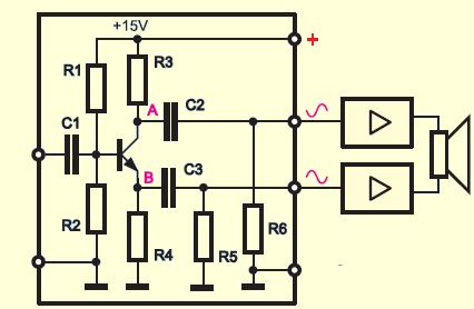
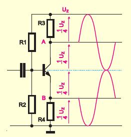
1) I read about the q-point at which he transistor must be set at dc operation before injecting the small ac signal to the base..the articles talking about the q point is always using a graph what is called the output characteristics curve including Vce on x-axis and Ic at y-axis...at different Ib......my question is that: is the graph is the same for all the transistors or every transistor have it's own values on that graph ...also is there any way else i can determine the q-point from the data sheet and if i must use the previous mentioned graph how could i get it because i didn't find it in the data sheet.
2) is the hfe (gain) constant for every transistor or it varies according to the bias..i mean that i read at a website that that gain is determined by the graph by the following way:
- determin that vce is half the vcc and from the graph at the
q point find the ic and corresponing ib and divide ic by ib
to give the gain.....is this true and if it is true does the
gain for the same transistor varies by varriyng the ic
and ib according to the determined q point first?
3)is it really right that the vce must be half vcc?or if using RE..is it right that Vce+Ve=half vcc...
4) is it right that Re must have 20% of the Vcc across it
5)is it right that the current flowing thought Rb1 , Rb2 must be 10 times the calculated ib
6) also how can i determine the value of the coupling capacitors Cin an Ce
7)how to calculate the max ac input
please i want the answers with simple effective explanation
thank you in advance
hi every one
i had searched a about the idea of biasing the transistor in the common emitter circuit
i had read different ways but am little confused about something that i want to ask about
1) I read about the q-point at which he transistor must be set at dc operation before injecting the small ac signal to the base..the articles talking about the q point is always using a graph what is called the output characteristics curve including Vce on x-axis and Ic at y-axis...at different Ib......my question is that: is the graph is the same for all the transistors or every transistor have it's own values on that graph ...also is there any way else i can determine the q-point from the data sheet and if i must use the previous mentioned graph how could i get it because i didn't find it in the data sheet.
2) is the hfe (gain) constant for every transistor or it varies according to the bias..i mean that i read at a website that that gain is determined by the graph by the following way:
- determin that vce is half the vcc and from the graph at the
q point find the ic and corresponing ib and divide ic by ib
to give the gain.....is this true and if it is true does the
gain for the same transistor varies by varriyng the ic
and ib according to the determined q point first?
3)is it really right that the vce must be half vcc?or if using RE..is it right that Vce+Ve=half vcc...
4) is it right that Re must have 20% of the Vcc across it
5)is it right that the current flowing thought Rb1 , Rb2 must be 10 times the calculated ib
6) also how can i determine the value of the coupling capacitors Cin an Ce
7)how to calculate the max ac input
please i want the answers with simple effective explanation
thank you in advance