Continue to Site

Welcome to EDAboard.com

Welcome to our site! EDAboard.com is an international Electronics Discussion Forum focused on EDA software, circuits, schematics, books, theory, papers, asic, pld, 8051, DSP, Network, RF, Analog Design, PCB, Service Manuals... and a whole lot more! To participate you need to register. Registration is free. Click here to register now.

Queries on gm/id methodology

Status
Not open for further replies.
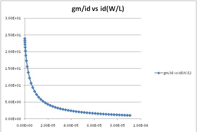
The transconductance efficieny (gm/ID) drops more rapidly for short channel devices due to velocity saturation.You can plot gm/ID versus current density ID/(W/L) for different channel lenghts to confirm this.The comparison should be made for same shape factor (W/L) and same ID apparently so that the conclusion makes sense.

As far as the ICMR you should study the respective equations (let's say from Gray-Meyer's Book) and then via trial and error simulations try to reach the spec.
 
@erikl:I'm attaching my gm/id vs id/(W/L) plot. If I choose a value of 10 for gm/id then my corresponding value of id/(W/L) is 72uA.
Ravinder: From your plot I get a value id/(W/L)≈7µA for gm/id=10 , not 72µA.

With bias current as 45uA(considering slew-rate requirements and power dissipation) my W/L should be less than 1 and with this value of W/L i will never achieve a gain of 100.
No. For 45µA you'd get a W/L=45/7≈6.4 .
 

It is 7.2E-005(72uA)

---------- Post added at 18:36 ---------- Previous post was at 18:29 ----------

ohh sorry i will recheck my graph

---------- Post added at 18:41 ---------- Previous post was at 18:36 ----------

@Erikl :but after setting W/L ratios how should I fix my input common mode voltage.Does gm/id plot vary with channel length.
In one paper I read it was shown that input swing as -1V to 1V.Will theren't be any linearity problems with such high swing
 

@Erikl :but after setting W/L ratios how should I fix my input common mode voltage.
Without more info about your circuit (schematic, op. voltage VDD) I can't help you further.

Does gm/id plot vary with channel length.
Only in strong inversion, not much in moderate and weak inversion, s. the 2 pages from David M. [Binkley]'s book "Tradeoffs and Optimization in Analog CMOS Design" (180nm process; separate plots for nmos & pmos). View attachment Binkley_gm_over_Id_for_diff_L.pdf
With gm/Id=10 your mosfet is still working in moderate inversion (IC ≈ 7).

In one paper I read it was shown that input swing as -1V to 1V. Will theren't be any linearity problems with such high swing
Depends on the process used and - by this - the usable op. voltage VDD. With VDD=5V a common input voltage range of 2V can easily be achieved. Neg. input voltages aren't possible on-chip anyway, they would have to be level-shifted or separated by SC method.
 

Depends on the process used and - by this - the usable op. voltage VDD. With VDD=5V a common input voltage range of 2V can easily be achieved. Neg. input voltages aren't possible on-chip anyway said:
My question isn't how we manage negative voltages but will the gain linear because input voltage swing is very high
 

My question isn't how we manage negative voltages but will the gain linear because input voltage swing is very high

Once again: "Depends on the process used and - by this - the usable op. voltage VDD. With VDD=5V a common input voltage range of 2V can easily be achieved." Anyone who can read is better off!
Input common voltage range means linear range!
 

I don't think so because as I think ICMR gives range of input voltage over which transistors are in active region and if the transistors are in active doesn't mean the gain would be same at every point in ICMR.Correct me if I'm wrong....
 

Input common voltage range means linear range!

I don't think so because as I think ICMR gives range of input voltage over which transistors are in active region and if the transistors are in active doesn't mean the gain would be same at every point in ICMR.Correct me if I'm wrong....

I think this is no contradiction: "linear range" doesn't mean the gain is totally constant over the ICMR - that's never the case. It's just another term for the CMR, which by convention is limited by a (-)3dB drop related to the max. gain, s. the foll. plot from a C@dence tutorial: View attachment CMR.pdf
 

Hi all,
I've designed two stage miller opamp using gm/id methodology.I had set gm1/id as 10 with id as 22.5uA,hence my gm1 is 225u.I've placed a compenstation capacitor(Cc) equal to 110f.So I should get GBW(=gm1/Cc) of 2GHz,but from AC analysis I'm getting only 220MHz.Can any body figure out the mistake I've made in my Circuit.

Thanks&Regards,
Ravinder.
 
Last edited:

Do the gm/id plots vary with channel length?Because I'm getting different gm/id plots for 100n and 300n.Here is the plot I'm attaching gmid plot for L=300n,earlier I've attached gmid plot for 100n

yes... i would suggest you do one with minimum length, 3* min L , 5 *min L. u can use the min L for input pairs and cascodes and the 3/5*min L for current mirrors.
 

@steadymind:Can you please explain me why the GBW is not coming out to be same as that of Handy calculations(gm1/Cc)!!
 

1. do u get gm1 to be 225u in your sim (u can look at gm in result browser for the corresponding mos).
2. how did u come to conclusion gm/Cc is the GBW. the 2 stage amplifier with miller cap. is a 2 pole system, the impedance that u see at the end of stage one will be miller cap will be multiplied by the gain of NM7 plus the output cap. so ur bw should be gm/(Cc*Avnm9 + cl)

looking at ur schematic , here are some tips
make the length of current mirrors atleast twice minimum length (if u plot i vs vgs/vds curves u will see the impedance difference).
try to match nm7 (width and length ) to nm0/nm1 this will improve matching and avoid unwanted vds mismatch and make the layout a lot lot easier.
 

2. how did u come to conclusion gm/Cc is the GBW. the 2 stage amplifier with miller cap. is a 2 pole system, the impedance that u see at the end of stage one will be miller cap will be multiplied by the gain of NM7 plus the output cap. so ur bw should be gm/(Cc*Avnm9 + cl)
I got GBW formula from text by Allen&Holberg.And at unity gain gain of th opamp must be 1 so Avnm9 may be equal to 1
do u get gm1 to be 225u in your sim (u can look at gm in result browser for the corresponding mos).
yeah it is around 240u.

make the length of current mirrors atleast twice minimum length (if u plot i vs vgs/vds curves u will see the impedance difference).
try to match nm7 (width and length ) to nm0/nm1 this will improve matching and avoid unwanted vds mismatch and make the layout a lot lot easier.
my channel lengths are 5 times minimum channel length.
 

Allen&holberg does quote GB = gm/Cc but i highly doubt this in practice. your gate cap of NM7 may contribute to this Cc. ie u may have Cc+ Cgate(NM7) dont know how big this will be. you can isolate this by adding a zero volt DC source at the gate of NM7. vary Cc and see how it affects ur GBW.
 

ie u may have Cc+ Cgate(NM7) dont know how big this will be.
yeah me too have same doubt whether to add overlap capacitance to Cc but even if add overlap capacitance(cgd) of both transistors(NM7 and PM10) to Cc it is coming out to be 245fF,yet my gm/(Cc+Cgd) is not close to what simulation value.
you can isolate this by adding a zero volt DC source at the gate of NM7.
Sorry,I couldn't get you
 

I am not sure what is exactly happening, i will try to simulate a 2 stage and let u know later today.. but for dc isolation look at he pic

17_1298396724.jpg
 
@SteadyMind:I've tried the method you suggested but there is no change in GBW(190MHz).
If I use this ota in Sample and hold circuit what is the max sampling rate I can operate?
 
Last edited:

the maximum sampling rate is determined by the R-C of the switch and how much sampling error u can tolerate. the settling time of the amplifier for the given load will decide if u can operate at a specified speed.

---------- Post added at 17:56 ---------- Previous post was at 17:53 ----------

what exactly are u trying to achieve.....
see this link https://www.ee.ucla.edu/~brweb/papers/Conferences/RCICC97_2.pdf and references 10,11.
 

Status
Not open for further replies.

Part and Inventory Search

Welcome to EDABoard.com

Sponsor

Back
Top