Continue to Site

Welcome to EDAboard.com

Welcome to our site! EDAboard.com is an international Electronics Discussion Forum focused on EDA software, circuits, schematics, books, theory, papers, asic, pld, 8051, DSP, Network, RF, Analog Design, PCB, Service Manuals... and a whole lot more! To participate you need to register. Registration is free. Click here to register now.

Pulsed RF Signal Modulator Spectrum Contamination Problem - Sideband

Status
Not open for further replies.

BorisBJL10

Newbie level 5
Newbie level 5
Joined
Jan 23, 2013
Messages
10
Helped
0
Reputation
0
Reaction score
0
Trophy points
1,281
Visit site
Activity points
1,372
Hi everybody,

I'm trying to prototype an exciter board for a pulsed beacon transmitter operating at 960-1000 MHz band.
I've built a board which uses two Hittite HMC221A switches employed as SPST pulse RF modulator after PLL and two amplifier stages
Switch operates at approx. +18 dBm power level.
The issue I've got is a pulsed RF signal spectrum sideband contamination, which is seen as an extra unwanted 'tail' of Fourier 'bells' at frequencies only below main signal, spanning for almost 50 MHz more that it should. Pulses are 6 uS wide and 1600 Hz PRF. Attached is a screenshot from spectrum analyzer, at 200 MHz span.
PLL sythesizer's CW signal before switch is totally and knowingly perfect.
I'd love to get your comments on possible causes of this issue. Where could this crap come from?

Thanks.
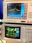
PulseSpectrum.jpg
 

I expect a feedthrough from the switch control, e.g. digital supply noise. GaAs switches have generally a poor isolation between switch control and RF path, so it might be necessary to explicitely filter out noise in the signal band.
 

I think one issue was presented above, a leakage of control pulses to RF. Another possible cause maybe is the SPST switch poor isolation due to the design. Using a SPST switch at 18 dBm may be the problem. Did you try to use the switch BEFORE the power amplifier? Try to vary input power and see how the spectrum changes.
 

Tested again and it seems like problem is in power amplifier path. Switch outputs relatively decent signal. It is fed into Freescale MW7IC930 30 W class AB amplifier IC and then into two-stage 1 kW class C RF PA (300 W and 1400 W Integra bipolar transistors). Some distortion is seen after 30 W amp and at 1 kW output it bad, the way it's on my picture.
Any ideas? Would it be worth to try collector pulse modulation at 30 W or 300 W stages? Could that affect spectrum?

BTW I tried to play with switch digital control path - placed RC networks there, that didn't do a thing, neither negative nor positive, no effect at all.
And I lowered RF power level at switch input by 2-3 dBm, that has no effect on spectrum either.

These high-power pulsed amplifiers rarely generate a pure spectrum. Yours looks good but some 40 dB down. Maybe it is time to use a band-pass filter. Pulse power amplifiers are never linear and adding pulsing to the power stage is often expensive.
 

These high-power pulsed amplifiers rarely generate a pure spectrum. Yours looks good but some 40 dB down. Maybe it is time to use a band-pass filter. Pulse power amplifiers are never linear and adding pulsing to the power stage is often expensive.

I don't think there are such BPFs, since I have to cover a band of 40 MHz with 60 channels.
Unless it is a tracking filter capable of handling over 1 kW of RF power )
 

Try looking at the AM to PM conversion in the class C amplifier, a degree or so per dB over the rise time of the signal will induce some FM sidebands.
 

If I were doing this, I would use this switch instead:
HMC284AMS8G

Is is non-reflective, so the PLL has a ~constant load impedance. With your reflective switch, unless you have it wired up as non-reflective with additional 50 ohm resistors...you are going to get frequency pulling whenever it switches. This might be the cause of your spurious signals. You may not notice this, because the pll will correct the frequency error in a few milliseconds, so in steady state it looks like the frequency is stable. In fact, your spectrum analyzer in your initial post looks just like that...at switching time (rf turning on) the frequency is too low, and the PLL eventually pulls the frequency a little higher.

Also, make sure your amplifier input has a decent return loss. Even with a non-reflective switch, the VCO may momentarily flip out if the amplifier input return loss is poor.

Also, any of these switches might have a DC pulse, maybe as high as 3 volts, coming out of the RF port at the moment it switches. A small inductor to ground and a small value (like 2 pF) series capacitor would fix that. Such a pulse might get into the power amplifier front end, and cause some interesting biasing effects.
 
Last edited:
  • Like
Reactions: FvM

    FvM

    Points: 2
    Helpful Answer Positive Rating
Firstly, I've got non-reflective switch design (two switches in series /RF2-to-RF2/ and two 51 Ohm resistors from RF1s to gnd, topology exactly similar to HMC-C019). Also, exciter board overall chain is: PLL (ADF4351), 2 dB attenuator, MCL PHA-1+ amplifier, then 10 dB attenuator, then again PHA-1+ amp, then 3 dB atten., switch, 2 dB atten. and then MW7IC930 30 W amplifier IC.
So I don't think reflections and pulling should be an inssue.

Most interesting thing is that this sideband on the left, which spans down to 900 MHz IS NOT MOVING anywhere, when I switch signal frequency, from 960 to 1000 MHz. It just stands there, like a cloud. It's steady. It is 'wide' when 1000 MHz signal and tightens when at 960 MHz.
 

I do not know your exact requirement, but last time I did something like that, I was surprised to calculate I needed 90 dB of one way isolation in the switch/amplifier/pad combination.
 

Most interesting thing is that this sideband on the left, which spans down to 900 MHz IS NOT MOVING anywhere, when I switch signal frequency, from 960 to 1000 MHz. It just stands there, like a cloud. It's steady. It is 'wide' when 1000 MHz signal and tightens when at 960 MHz.
Does the sideband depend on the power of the pulse applied? If you shut off the RF entirely and operate the switch does the sideband remain?
You may want to look at whether the various PA stages have stable biasing during the pulse.
 

Switch outputs a signal that has this sideband but at much lower levels - about -75 dBc.
Last two RF stages are classs C bipolar transistors, so obviously there is no any bias invoilved there. 30 W pre-amplifier is biased in class AB - 100 mA and 250 mA currents in its internal stages..

As for PLL isolation, in ADF4351 VCO does not drive RF path directly. It uses digital divider by 4, so I guess it does not give any damn about frequency pulling and isolation.

Sideband goes up and down with RF power change, respectively.

Is it worth trying closing switch for good and try collector modulation, by pulsing DC power supplies to 30 W pre-amplifier and/or output RF transistors?
 

I don't know if you have the possibility to change the shape of the pulse using a raised-cosine filter with acceptable bandwidth and roll-off factor, to meet the other system requirements. I think this would solve the most of the spectrum problems.
 

UPDATE:
Spent all night in the lab - here's what happening.
Switch provides perfect output, symmetric, no distortion. All junk & garbage is being born in that 30 W amplifier IC (MWIC930NR or MW7IC930NR).
It is the one which adds that sideband, at -60 dBc level. When signal is fed into two stage class C 1 kW power amp sideband reaches -50 dBc level. But if it won't be there after 30 W stage in the first place, I guess it won't be in high power stages either.

I think I will have to switch ideology to 'collector modulation' type of pulsing and omit the switch completely. Here's what I did today.
I've applied constant +5 VDC to switch data input, thus opening it for good, and pulsed 2nd stage of MWIC930NR IC through IRF5210 P-Ch FET driver, being driven with Zetex ZXMN7A11 N-Ch FET controlled with 5V logic digital data input from pulse source.
I've got very clear and narrow spectrum, but very slow rise & fall times (400 ns and 1000 ns respectively), so I need to design or get a ready-made very fast power complementary driver, which would be driven with CMOS +5V logic and output fast 28 V pulses (<= 100 ns rise and <=300 ns fall), being able to provide 4-5 amps of pulse current into 500-1000 pF load.
Do you know such driver ICs? I can't find any. Is discrete FETs design the only option here?
 
Last edited:

Check out IXDD614 and IXDD630 and other parts in that family. Drive voltages up to 35V, continuous currents up to 8A and switching times <100ns. Probably the most rugged driver ICs I've ever worked with. I've never used them to bias RF amps though, might want to put a small LC filter on the output.
 

Status
Not open for further replies.

Similar threads

Part and Inventory Search

Welcome to EDABoard.com

Sponsor

Back
Top