Continue to Site

Welcome to EDAboard.com

Welcome to our site! EDAboard.com is an international Electronics Discussion Forum focused on EDA software, circuits, schematics, books, theory, papers, asic, pld, 8051, DSP, Network, RF, Analog Design, PCB, Service Manuals... and a whole lot more! To participate you need to register. Registration is free. Click here to register now.

problem on LDO ac simulation.

Status
Not open for further replies.

ken_cn

Member level 2
Joined
Oct 9, 2005
Messages
45
Helped
5
Reputation
10
Reaction score
3
Trophy points
1,288
Activity points
1,648
Hi all,

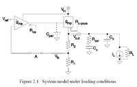
I am doing the ac simulation of a LDO. I used the method which was mentioned in the thesis of Rincon Mora (see the following Fig.)
But in my simulation I found that the output voltage is changing in defferent load conditions, and sometimes even at minus values. So I think the on-res of the pass element is not make sense.
My question is how to maintain the output voltage at the value it was used (i.e. 3v or 5v)?
Thanks
!
 

Did you check in advance if there is a correct bias point for doing an ac analysis ?
 

Yes.
THe bandgap and amp is at the correct operating point.
Then minus voltage is because of the Loading current source which is connecting to the output of the pass element directly.
 

It is not easy to give a substantial answer bacause
- the function and properties of the pass element are not known ,
- the value of the on-resistor is not known.

More than that, the method of the loop gain simulation cannot be derived from the figure - only the point of cut can be seen.
 

ken_cn said:
Yes.
THe bandgap and amp is at the correct operating point.
Then minus voltage is because of the Loading current source which is connecting to the output of the pass element directly.

it looks like ur pass transistor size is not enough......
 

can you reveal some more details... about what and how you are trying to do?

some schematic...?
 

It depends on how you are breaking the loop .. Use a low pass filter
to break the loop with large R and C values .. that way you can
isolate the DC and AC signals ..

Raduga
 

Oh no, don´t do this. There are much better alternatives than this crude method.
 

hello

just place vdc source with 0 DC between vfb and "-" input and run stb analysis in spectre pointing this source

regards
 

If using hspice then its better to use a large inductor to break the loop and a large capacitor to inject ac signal...(this is yet crude)

best is to go with middlebrook method provided you have the patience to implement it in hspice.
 

Yes, the Middlebrook method is most exact and can be applied always - and that´s what SPECTRE has incorporated.
However, in many cases it is sufficient to break the loop and to place a voltage source between (i.e. in series) both ends (A) and (B).
Then, all bias conditions are preserved and the loop gain is calculated simply by LG=V(B)/V(A). The only drawback of this simple method is, that it works errorless only if there is a point which does not change load conditions - for example: opamp inputs ore output. Very often I have applied this simple loop gain method.
 

Thanks all.
Could you tell me what is the "Middlebrook method"? And how to simulate in spectre.
 

ken_cn said:
Thanks all.
Could you tell me what is the "Middlebrook method"? And how to simulate in spectre.

According to Middlebrook, two open loop simulations are to be performed - and combined with each other. One simulation with a voltage source and another one with a current source. The formulas can be found elsewhere (google for "middlebrook").
 

agree with rajanarender_suram
 

Hi rajanarender_suram & paley.
Could you tell me why a small size pass element can cause this result?
My pass element's size is 100u/0.5u by 80 to handle 50mA load current. And the dropout voltage is 100mV at 50mA. I think it is large enough.

B.R.
Ken
 

I think it is a bit small... though it depends on the technology you are using...

but something like (100/0.5 )*100 would do better.
 

you can use a resistor and a capacitor to bread the loop.

: ----R=1G----------------AC source--------
: ~~~~~~~~ |
: ~~~~~~~~ |
: ~~~~~~~~ C=1G
: ~~~~~~~~ |

See a book wirte by allen. The way to bread AC loop is discribed in the chapter of OPAMP.
 

Try the method by LvW. Do not try LC or RC method. For more details, you can refer to "The Designer's Guide to SPICE and Spectre"
 

ken_cn said:
Hi rajanarender_suram & paley.
Could you tell me why a small size pass element can cause this result?
My pass element's size is 100u/0.5u by 80 to handle 50mA load current. And the dropout voltage is 100mV at 50mA. I think it is large enough.

B.R.
Ken

first diode connect ur Pmos pass and connect the S terminal to Vin and G/D terminal to Gnd. and do DCop analysis.. u will find that Ids of the PMOS is less than 50mA as this is the case of highest (Vgs-vt)...if thats the case than how come the transistor draw 50mA with less (Vgs-Vt). so some of the nodes should misbehave in the simulation......
 

Status
Not open for further replies.

Part and Inventory Search

Welcome to EDABoard.com

Sponsor

Back
Top