Continue to Site

Welcome to EDAboard.com

Welcome to our site! EDAboard.com is an international Electronics Discussion Forum focused on EDA software, circuits, schematics, books, theory, papers, asic, pld, 8051, DSP, Network, RF, Analog Design, PCB, Service Manuals... and a whole lot more! To participate you need to register. Registration is free. Click here to register now.

Practical question about SMA on PCB

Status
Not open for further replies.

antenna_abc

Member level 3
Joined
Dec 22, 2005
Messages
58
Helped
0
Reputation
0
Reaction score
0
Trophy points
1,286
Activity points
1,835
edge-launch sma

Hi, everyone. I have a practical question about mounting a SMA connector on a multilayer PCB.

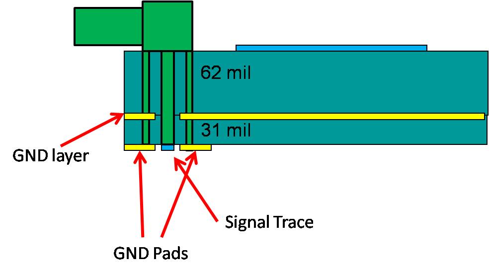
The PCB has two substrate and 3 copper layer, with top and bottom as signal layer, and intermediate as GND layer. And I want to mount the SMA connector on the PCB, with the signal pin connected to the bottom signal layer, as shown in the attachment.

The problem is that the PCB itself is too thick for the edge-launch SMA connector in attachment (a). And since the GND layer is sandwiched by two substrates, it is also very difficult to insert the PCB to the SMA connector slots.

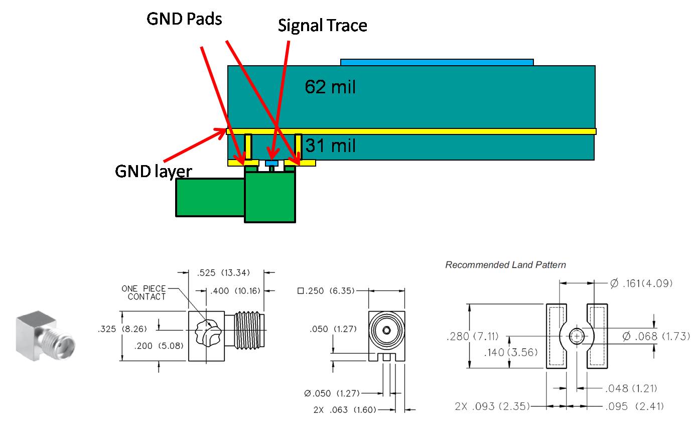
So I am going to use the thru-hole SMA in attachment (b). My question is how to ensure the signal pin and the GND pins are electrically connected to the PCB? Does anyone have the idea about how to make the PCB layout and via holes for this thru-hole SMA connector for multi-layer PCB?

Thanks.
 

sma on pcb

Use a connector like this one, and come into the board from the opposite side that the signal trace is on. Will work up to board thickness of .125". You will want 5 plated thru holes drilled, one for the signal, and four for the ground plane connection, with five surface round pads on the signal side for a good solder fillet.

http://www.smelectronics.us/SC8252.pdf

BTW, what freqency? That board will be pretty lossy.
 
sma pcb connector layout details

Thanks, biff44.

My board is only working on 1GHz, so FR4 is fine. I have attached a picture for using the thru-hole SMA connector as you mentioned. Would you check that is correct or not?

If possible, would you also recommend the PCB pads layout for me? Thanks


sma pad pcb

I have faced similar issues.

The key is that you are operating at 1 GHz and at this relatively low frequency it will be hard to screw up the works.

Another advantage to the mount you are considering is that it will be harder to tear the connector off the board,

Recommended footprints are hard to come by as most connector manufacturers sell you connectors and wish you good luck when it comes to actually using their parts. I would spend some time with HFSS to develop a footprint that worked if I was doing this work.

You may find that trimming the center (signal) pin close to the signal trace helps the match. The ground pins did not seem to need the trim.

I would also pay close attention to the trace width vs the center pin diameter of the connector you select to minimize the opportunity for a reflection.
 
sma to pcb

Hi, Azulykit. Thanks for your response and shares.

So if the frequency goes up, do you think this kind of thru-hole SMA connector will introduce extra parasitic inductance to the connections? And it cannot be used?

The other SMA connector I found is attached in this post. It is surface-mounted type. Do you think it will help to reduce the parasitic at high frequency?

The only problem for me to use the surface-mounted SMA is I don't know how to solder it to the pads, since I think the inner signal pin is blocked by the GND walls. I am wondering whether there is anyone would recommend some soldering techniques for hand-made prototyping?

Thanks.


sma pcb connector footprint

The board thickness will lead to multimoding problems as the frequency gets higher, so the only solution is to make the board thinner. You might get away up to 2.4 GHz, since your effective board thickness for the RF is only 31 mils.

The connector problem is that the center pin has a lot of inductance in series with your signal path, and any solder pads have shunt capacitance to ground. If you draw out that circuit, you will find that it looks just like a lowpass filter. And like any lowpass filter, there are two issues: you want the input/output to be matched to 50 ohms, AND you want the cutoff frequency to be well above your operating frequency.

So you try to minimize the stray reactances as much as possible, and try to make the stray reactances form a "matched" 50 ohm structure. Often time this leads to necking-down the trace before it gets to the center pin, and adding a bigger pad at the center pin solder connection--in other words leading into the whole mess with a series inductance and then deliberate shunt capacitance right where the connector starts in order to fill out the remaining portions needed to form a matched lpf stucture. I do not have the details for you, but you might search on google for "microstrip vias", or somthing like that, to get you started.

Added after 15 minutes:

Here is what I mean. The top image is what you are stuck with. The bottom image is what you do to the matching structure to form a matched LPF.
 
sma to pcb connectors, how work

I made an SMA work to around 6 GHz using the techniques above. By the way it was hand soldered to the PCB. Nothing exotic.

I would model the situation in HFSS to see the specific items selected worked together. That or lots of time in the lab with test samples. Anything else is just hand waving as far as a specific solution. (My comments included!)

As far as an upper limit I would get nervous about this as I got closer to Ku band frequencies. There night be problems at X as well. Model it or find someone to do it for you is my recommendation (if the application is critical).
 
Kazim,

There are numerous manufacturers who I am sure would easily make specification sheets available. Try southwest Microwave or Huber Suhner if you want good ones.


Regards,

Eb
 

Hi,
I have a less complicated problem. I would like to feed a 50Ohm microstrip using a SMA through hole connector from underneath the ground plane. I did a simulation for it using hfss. It happen that it isn't a good way to do. The return loss is getting worst at higher frequency. I am wondering why.
Thanks

---------- Post added at 16:28 ---------- Previous post was at 16:27 ----------

Forget to post the image


Because of microstrip-coaxial transistion...It's normal for your structure..
 

Because of microstrip-coaxial transistion...It's normal for your structure..
Basically, yes. Are you sure, that the other end of the transmission is perfectly matched? You may want to check by replacing the angled transition by something different for reference. Or use two of them.

You can however slightly reduce the discontinuity by adjusting the shape of the microstrip end.
 

Yes, I tested the line with two brick pec with waveport at the inner surface. The return loss and insertion loss is good as expected.
 

Status
Not open for further replies.

Part and Inventory Search

Welcome to EDABoard.com

Sponsor

Back
Top