Continue to Site

Welcome to EDAboard.com

Welcome to our site! EDAboard.com is an international Electronics Discussion Forum focused on EDA software, circuits, schematics, books, theory, papers, asic, pld, 8051, DSP, Network, RF, Analog Design, PCB, Service Manuals... and a whole lot more! To participate you need to register. Registration is free. Click here to register now.

Power MOSFET (SPB160N04S2L-03) footprint using Altium

Status
Not open for further replies.

Hanooda

Newbie level 5
Joined
Sep 18, 2012
Messages
8
Helped
1
Reputation
2
Reaction score
1
Trophy points
1,283
Activity points
1,337
Good Afternoon , how's every body?

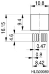
I want to get your feedback on my first footprint drawing using Altium Designer for Power MOSFET (Type: SPB160N04S2L-03) (Package:p- TO263 -7-3).
In the attchement you will find the altium footprint file. I used the PCB Layout Reference View which was provided in the datasheet to draw my footprint.
Could you check if my drawing have some mistake or not.

Looking Forward to hearing from you.
Hanooda
 

Attachments

  • SPB160N04S2L-03.gif
    SPB160N04S2L-03.gif
    5.7 KB · Views: 92
  • SPB160N04S2L-03.rar
    6.4 KB · Views: 58

Hanooda,
can you send in zip file, please
thanks,
keyur
 

Hi,
Hanooda, it looks correct to me, as you have got the footprint from the link below,

**broken link removed**

You have also done correct by removing the middle pin,
sometimes, you could order a dummy component from the supplier, and then check against the 1:1 copy of your gerbers.
thanks,
keyur

- - - Updated - - -

Hanooda,
I also checked the designator of the pads, which are not correct, they have 4th pin as tab, so generally internally connected to ground ( heat desipating pad) , so try to keep that in mind, you only have configued as six pads .
thanks,
keyur
 

Status
Not open for further replies.

Part and Inventory Search

Welcome to EDABoard.com

Sponsor

Back
Top