Continue to Site

Welcome to EDAboard.com

Welcome to our site! EDAboard.com is an international Electronics Discussion Forum focused on EDA software, circuits, schematics, books, theory, papers, asic, pld, 8051, DSP, Network, RF, Analog Design, PCB, Service Manuals... and a whole lot more! To participate you need to register. Registration is free. Click here to register now.

PIN diode switch in ADS

ET1990

Newbie
Joined
Feb 16, 2024
Messages
2
Helped
0
Reputation
0
Reaction score
0
Trophy points
1
Activity points
34
Good evening to all,
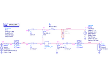
I just started to work with ADS, and so I am trying to reproduce a RF switch with PIN diode reported in this application note of the Infineon (pag. 12). This represents a real and working demo board. I took the parameter of the PIN diode from the SPICE model available at this URL and I copied them into the schematic.
schematic.png


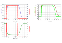
After the verification of the biasing with a “DC” simulation, I tried an “Envelope” simulation adopting a sinusoidal voltage source at the input of the switch and a step voltage source as control signal, but, as you can see, the behavior is not the expected one (there is no switching).

envelope1.png


I saw the same result also with the "Transient" simulation. On the other hand, I saw that substituting the inductors and capacitors with their ideal counterparts “DC feed” and “DC block”, respectively, the result of the “Envelope” simulation is the expected one (even if the isolation is poor).

envelope2.png


However, the "Transient" simulation shows again no switching. I made a lot of trials but I am not able to get the expected results with the complete circuit. Any suggestion? Thank a lot
 
Solution
Try skyworks PIN diodes for Attenuator.
End of this page, there is a ADS archived file and you can use those models for your purpose.
I have tested one of them and the result is quite promising. At least, you can see the isolation and insertion loss correctly.
Forget about DC Simulation it won't work.
You have to do a Small Signal simulation e.g. s-Parameters Simulation is enough.
Transient should work but Envelope Simulation has no function here.
Your target is to see Insertion Loss right ?? So do not dive into simulation details.
Also, R2=50 Ohm here and this is much larger than PIN Diodes Internal ON state resistance. Your set-up is wrong.
Thanks a lot for your reply! Beyond the insertion loss, I would like to see the switching in time-domain. This is why I am trying to use the Transient or Envelope simulations. So are you saying that a time-domain simulation is not possible with this kind of circuit? And if the answer is yes, why does this happen?
About the R2=50 Ohm, I set this value because in the demo board of the Infineon the common value of 50 Ohm is assumed for the input port. Why is this a problem? Thanks for your kind help
Time Domain Analysis is surely possible but this circuit will-probably-work under small signal conditions and therefore you should analyze this then check transient regime.
 
Last edited:
PIN diode switches operate as variable capacitors but they
are not capacitors, in the sense that there is DC conduction
possible in and near the "on" state. You need blocking caps
and you need both series and shunt, to get both low insertion
loss (on) and high impedance (off). The control voltage / current
must be inductor-blocked well out of band. Off state requires
high reverse voltage (>> amplitude) and On state requires
significant current (>> amplitude / 50 ohms).

With only the series switch, there can be still significant
through-signal that the L2 will not shunt, so through the cap
to the load.

This is not really any different than RF CMOS switches, if you
want isolation then you need both an "off" series and "on"
shunt(s). T or pi network depends on what your source looks
like, and are other things attached to it, and whether burning
RF input power when blocking seems like a good idea.
 

    ET1990

    Points: 2
    Thanks a lot for your analysis
I have checked this PIN Diode in a simple Small signal Simulation and found that the Insertion Loss under zero bias is not correct regarding to Datasheet.
Either the model itself is not correct or datasheet has an error.
 

    ET1990

    Points: 2
    Thanks! I will try another PIN diode in a different schematic
Try skyworks PIN diodes for Attenuator.
End of this page, there is a ADS archived file and you can use those models for your purpose.
I have tested one of them and the result is quite promising. At least, you can see the isolation and insertion loss correctly.
 

Attachments

  • PIN_Diode.png
    PIN_Diode.png
    136.6 KB · Views: 72
  • PIN_Diode_Output.png
    PIN_Diode_Output.png
    99.1 KB · Views: 74
Solution

LaTeX Commands Quick-Menu:

Part and Inventory Search

Welcome to EDABoard.com

Sponsor

Back
Top