Continue to Site

Welcome to EDAboard.com

Welcome to our site! EDAboard.com is an international Electronics Discussion Forum focused on EDA software, circuits, schematics, books, theory, papers, asic, pld, 8051, DSP, Network, RF, Analog Design, PCB, Service Manuals... and a whole lot more! To participate you need to register. Registration is free. Click here to register now.

PIN-diode controlled variable attenuator

Status
Not open for further replies.

imuuu_imran

Newbie level 6
Joined
Sep 22, 2009
Messages
14
Helped
1
Reputation
2
Reaction score
1
Trophy points
1,283
Location
sweden
Activity points
1,381
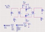
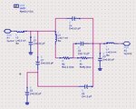
I am trying to build a PIN diode controlled variable gain attenuator by using two branch line directional coupler for my master's thesis at 7.5 GHz. In one journal they made such attenuator from 0dB coupler**broken link removed**. I have to use branch line instead of 0dB coupler. I need a schematic diagram for that with the controlling circuit of the pin diode. I have made a branch line directional coupler in ADS. 1.jpg I have tried to find a s2p file for PIN diode but unable to find one. at the end I found a ADS sub-circuit of the PIN diode Agilent HSMP-3810 in the internet but I don't know it is right or wrong.2.jpg. Also I need to know this sub-circuit is ok or not? Can some one help me?? :sad::cry:
 

It is not clear what topology you are planning on using, so draw a schematic of the full thing for us. If you are planning on using pin diodes as in that paper you referenced, you need a S1P file.
 
As you need a driver, you will need a simple variable current source to push through your PIN diode a DC current, from zero to a maximum specified current value.
Usually any variable voltage regulator can be used, with a series resistor set to limit the current at a maximum voltage it can reach.
The VVA response is not linear, it typically rises fast from zero mA , then slower to a maximum at e.g. 50 mA.
The maximum DC current usually depends on a maximum RF power your device should control; it is specified for a particular PIN diode.

Drivers recommended by VVA makers typically use opamps with a diode in feedback, in an attempt to linearize the response. You can play with many such circuits, or, you can design a DAC to get the current by a code to get a linear loss response.
 
Hi,

thanks a lot for the handbook.a :smile: This is the schematic that I have planed for this circuit. Untitled.jpg . Can anyone suggest me any site from where I can get my S1P file for the PIN diode. One more thing. is there any need to implement a RF choke in the PIN diode biasing circuit?
 

Hard to get S1P for a PIN diode. Usually the simulators use the Spice models for PIN diodes.
NXP have S-parameters for some PIN diodes, but they are not presented in a table format.
**broken link removed**

The choke is definitely necessary for the bias circuit. The topology of the bias is important for getting the best performances over wide frequency range.
https://www.skyworksinc.com/uploads/documents/200312C.pdf
 
Thanks vfone for your valuable comments. I made a RF choke for 7.5GHz and implemented it in the circuit. but I think I got nothing in the output port but strangely I am getting attenuation in the port which should be isolated (4). can I get any suggestion from you now?

schematic :Capture.JPG
output: Capture2.JPG
 

For 6-9GHz, you should connect all components with micsrostrip lines, and tune the lengths of the lines, to get your results.
 
Thanks vfone for your valuable comments. I made a RF choke for 7.5GHz and implemented it in the circuit. but I think I got nothing in the output port but strangely I am getting attenuation in the port which should be isolated (4). can I get any suggestion from you now?

schematic :View attachment 57646
output: View attachment 57647

If I were you, I'd design a PI or TEE circuit between two couplers.Because you change the characteristic impedance between these two couplers by connecting a single PIN diode and as a result your attenuation becomes nonlinear or irregular.Instead, using a PI or TEE attenuator between two couplers by maintaning the actual charateristic impedance will much better.
You can consider the attenuator circuits as TEE or PI resistive attenuator circuits with fixed input and output impedance.
 

Attachments

  • 200312C.pdf
    1.5 MB · Views: 147
  • chapter 3.pdf
    262.7 KB · Views: 231
Last edited:
Perhaps better choice is using different topology for the PIN network, but you can make it work even this one if you add DC blocking capacitors on each port.
Also place a resistor in series with each λ/4 transmission line (~500 ohms).
 

Hard to get S1P for a PIN diode. Usually the simulators use the Spice models for PIN diodes.
NXP have S-parameters for some PIN diodes, but they are not presented in a table format.
**broken link removed**

The choke is definitely necessary for the bias circuit. The topology of the bias is important for getting the best performances over wide frequency range.
https://www.skyworksinc.com/uploads/documents/200312C.pdf

Hello, I am simulating PIN diodes in ADS could you help me with the DC biasing circuit topology? Thank you.
 

Status
Not open for further replies.

Part and Inventory Search

Welcome to EDABoard.com

Sponsor

Back
Top