san94
Newbie
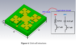
I am attempting to simulate a unit cell utilizing a Floquet port. The unit cell contains a pin diode that operates in two states. This diode is connected to the ground via a metal via hole and also includes a bias line. What is the correct procedure to simulate this configuration?
Initially, I attempted to design the pin diode based on its equivalent circuit using lumped elements, specifically a rectangular surface with boundaries assigned as lumped elements. However, the simulation did not show any noticeable change in the S-parameters when compared to the unit cell without the diode.
Considering the entire setup from a circuit perspective, the bias line is connected to a controller. One end of the diode is connected to the ground, completing the circuit. For the simulation, I intend to use the equivalent circuit for a single stage (on/off) and thus, I believe the bias line may not be necessary. In this scenario, would the circuit be complete?
I have come across some demonstrations of pin diode design within a transmission line, where both ends of the transmission line have lumped port excitations. I'm also curious to know if any modifications are required when using a Floquet port for this purpose.