jovin555
Advanced Member level 4

- Joined
- May 20, 2012
- Messages
- 115
- Helped
- 0
- Reputation
- 0
- Reaction score
- 0
- Trophy points
- 1,296
- Activity points
- 2,036
I am new to pic asm coding.i am trying to do a simple addition in asm.but its not working.can anyone tell me the reason
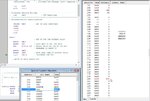
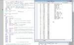
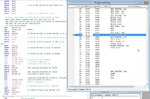
Code:
        list       F=inhx8m, P=16F877a, R=hex, N=0
	#include P16F877a.INC ; PIC definitions
	 __config _HS_OSC & _WDT_OFF & _LVP_OFF;
	; __config _config2,_IESO_OFF & _FCMEN_OFF
	;Errorlevel -302      ; switches off Message [302]: Register in operand not in bank 0.
	org		0x00
	goto	start
; Interrupt Service Routine -----------------------------------------------
;	org     0x04               ; ISR beginning
; -------------------------------------------------------------------------
; Microcontroller initialization
	org 	0x30
start:
	clrw
	clrf 	0x01
	clrf 	0x02
	clrf 	0x03
	movlw 	0x04
	movwf 	0x01
	movlw 	0x05
	movwf 	0x02
	addwf 	0x01,0x03
	NOP
	NOP
        end             ; end of program