glias
Full Member level 2
Hello all,
I would want to extract from my pcb some nets to check the level of LVDS pairs...
Since this pair is provided by a digital board, I have on my board only a connector then a resistive splitter and then 6 ADCs LVDS inputs.
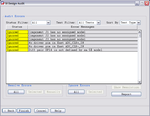
I have the ibis model of the adc input but when I want to create the topology it doesn't work well : PCB SI just tell me that there is an error.
It may come from the model assignement, could you please help me to assign correctly the model of the ADC... ? and for the connector, how can I do since I don't have model (in fact I would want to add in sigXplorer an ibis model of the FPGA ouput from the digital board).
I hope that someone could help me
thanks
