fasishah001
Newbie level 6
salam
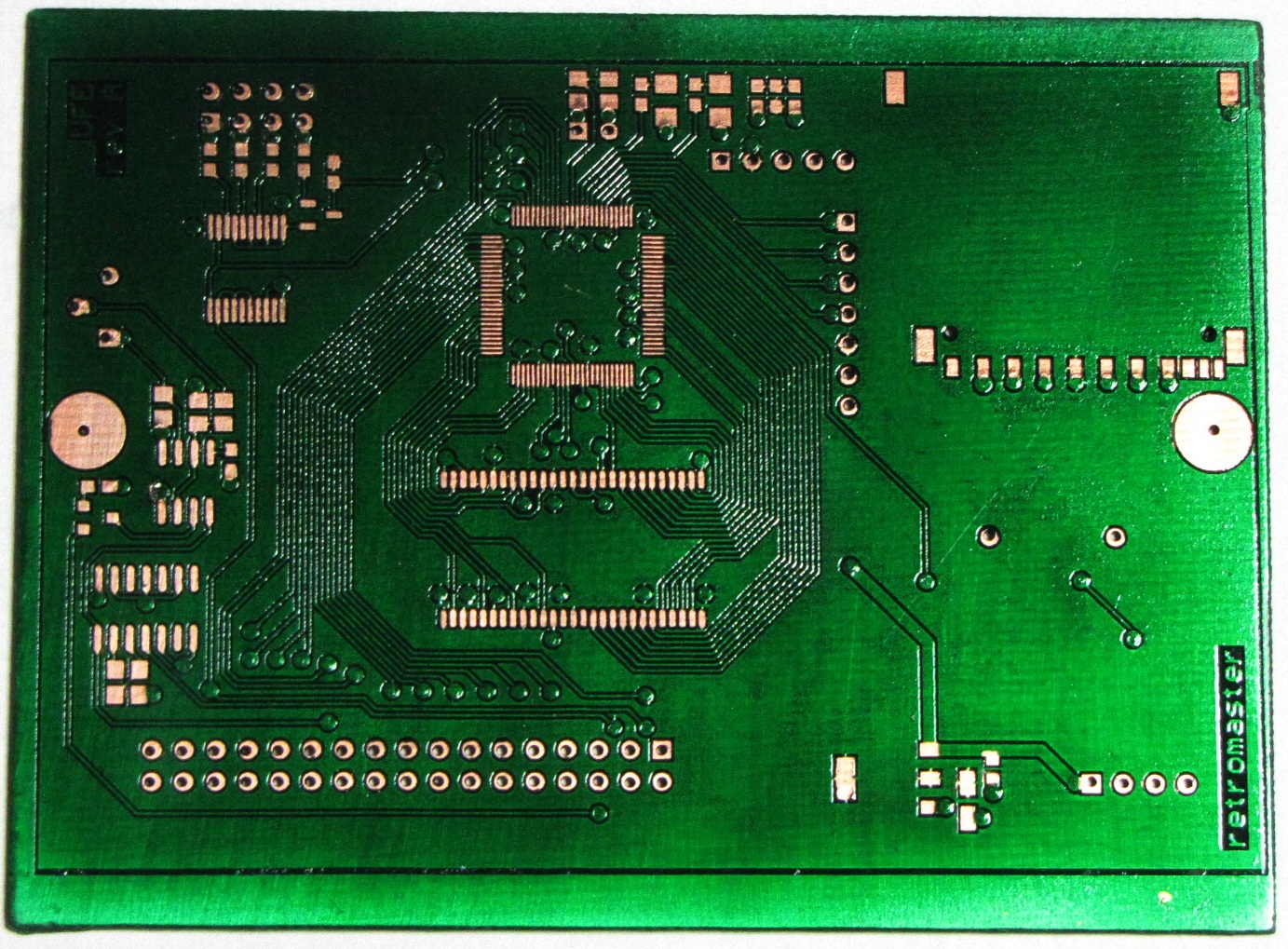
I wanted to know what is the green color coating that is done on the PCB called as? Is it to prevent oxidation of copper??
I have etched my own PCBs using toner transfer method.Is it really necessary to apply the green coating on the exposed copper?
I will use silicon layer so its enough or not??
Thanks.