Continue to Site

Welcome to EDAboard.com

Welcome to our site! EDAboard.com is an international Electronics Discussion Forum focused on EDA software, circuits, schematics, books, theory, papers, asic, pld, 8051, DSP, Network, RF, Analog Design, PCB, Service Manuals... and a whole lot more! To participate you need to register. Registration is free. Click here to register now.

OTA Design for Band Pass Filter Applications

Status
Not open for further replies.

sci-fi_guy

Newbie level 4
Joined
Sep 9, 2017
Messages
5
Helped
0
Reputation
0
Reaction score
0
Trophy points
1
Activity points
43
Hello,

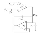
I am trying to design an Operational Transconductance Amplifier (OTA) to be used in the following band pass filter (C4 BPF):
C4.JPG

It has the following transfer function:

C4 e1.JPG C4 e3.JPG C4 e2.JPG C4 e4.JPG

Both Gm1 and Gm2 are subthreshold transconductances.

What is the most suitable OTA design/architecture for this filter and how should I select the transistor W/L's?

I am using Cadence with AMS 0.35um 4 metal process (c35b4) technology.
 

How will you keep constant the subthreshold tranconductances under larger signals? Even in saturation it is complicated. If you want to keep the devices in subthreshold then you should use very high W/L for input devices, to keep area and input capacitance low use minimal length.
 
I'd use one of the simplest 2-stage-OTA configurations, n- or p-input:
2-stage_n-input_OTA_principle.jpg 2-stage_p-input_OTA.jpg

W/L ratios depend on necessary current, and this latter one depends on required bandwidth and actual load capacitance.
 
Status
Not open for further replies.

Similar threads

Part and Inventory Search

Welcome to EDABoard.com

Sponsor

Back
Top