Continue to Site

Welcome to EDAboard.com

Welcome to our site! EDAboard.com is an international Electronics Discussion Forum focused on EDA software, circuits, schematics, books, theory, papers, asic, pld, 8051, DSP, Network, RF, Analog Design, PCB, Service Manuals... and a whole lot more! To participate you need to register. Registration is free. Click here to register now.

[SOLVED] On resistance of nmos switch and transmission gate

Status
Not open for further replies.

Saraadib

Member level 4
Joined
Nov 2, 2015
Messages
78
Helped
0
Reputation
0
Reaction score
0
Trophy points
6
Activity points
1,116
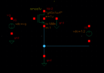
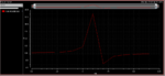
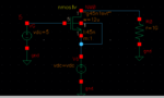
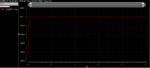
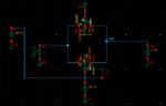
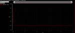
I want to measure on resistance of nmos and transmission gate ,I know on resistance is resistance of transistor when transistor is in triode region
I have attached schematic of nmos transistor and transmission gate and plot on resistance of both, however result of them is wrong
Does any body have idea what is wrong with my circuit?
 

Attachments

  • 7.PNG
    7.PNG
    9.1 KB · Views: 520
  • 8.PNG
    8.PNG
    15.9 KB · Views: 508
  • 9.PNG
    9.PNG
    9.4 KB · Views: 589
  • 10.PNG
    10.PNG
    15.5 KB · Views: 514
Last edited:

For the 1st two images (7.PNG & 8.PNG) it is not clear (for me) if the nmos is closed or open, because vdc of V6 isn't given.

For the 2nd two images (9.PNG & 10.PNG) both nmos and pmos transistors are heavily "on" (switch closed), yet it is not clear which voltage (if any) is provided by V0. But anyway the low switch resistance of a few tens or hundreds of Ohms should be shown, as the impedance of V0 is zero. I guess the ordinate's scale of 10.PNG is GOhms, isn't it?

in 1 two image(7 and 8 PNG),I sweep vdc of v6 from 0 t0 5V and plot output voltage which voltage at resistance(1G) and subtract it from input voltage which is V6 and divided on Current of nmos
can you please tell me how exactly I have to do for measuring on resistance of switch?
how should I change my circuit to see on resistance of switch
Yes,ordinate's scale of 10.PNG is GOhms
 

For the 1st two images (7.PNG & 8.PNG) it is not clear (for me) if the nmos is closed or open, because vdc of V6 isn't given.

For the 2nd two images (9.PNG & 10.PNG) both nmos and pmos transistors are heavily "on" (switch closed), yet it is not clear which voltage (if any) is provided by V0. But anyway the low switch resistance of a few tens or hundreds of Ohms should be shown, as the impedance of V0 is zero. I guess the ordinate's scale of 10.PNG is GOhms, isn't it?
in 1 two image(7 and 8 PNG),I sweep vdc of v6 from 0 t0 5V and plot output voltage which voltage at resistance(1G) and subtract it from input voltage which is V6 and divided on Current of nmos
can you please tell me how exactly I have to do for measuring on resistance of switch?
how should I change my circuit to see on resistance of switch
Yes,ordinate's scale of 10.PNG is GOhms
 

in 1 two image(7 and 8 PNG),I sweep vdc of v6 from 0 t0 5V and plot output voltage which voltage at resistance(1G) and subtract it from input voltage which is V6 and divided on Current of nmos
This can't work as here the current is determined by the much higher load resistor of 1 GOhm.
You better put V6 as a fixed voltage source (e.g. 5V) between drain and vdd (i.e. it creates vdd), no load resistor in between, sweep VG between 0 and 5V, and plot vdd divided by the nmos current. Use an ordinate's scale of Ohms, then you should see the nmos' resistance falling from an initially high value below the threshold voltage vth, after exceeding vth it should go down to several hundreds or tens of Ohms when increasing VG up to 5V.

Yes,ordinate's scale of 10.PNG is GOhms
Similar for the 2nd two images 9 & 10.PNG: With a load resistance of 1 GOhm you can't see the much lower transmission gate (TG) resistance. Remove R0 and connect vout to vdd/2. In your configuration the TG is always on (switch closed). Sweep the input voltage V0 from 0 to 5V and plot vdd/2 divided by the current through V0 (which equals the total current through the TG). Here again use an ordinate's scale of Ohms[/U], and you should see the low TG resistance (should look like a Vesuvius: peak near vdd/2 , s. e.g. any 4016|4066 data sheet).
 
This can't work as here the current is determined by the much higher load resistor of 1 GOhm.
You better put V6 as a fixed voltage source (e.g. 5V) between drain and vdd (i.e. it creates vdd), no load resistor in between, sweep VG between 0 and 5V, and plot vdd divided by the nmos current. Use an ordinate's scale of Ohms, then you should see the nmos' resistance falling from an initially high value below the threshold voltage vth, after exceeding vth it should go down to several hundreds or tens of Ohms when increasing VG up to 5V.


Similar for the 2nd two images 9 & 10.PNG: With a load resistance of 1 GOhm you can't see the much lower transmission gate (TG) resistance. Remove R0 and connect vout to vdd/2. In your configuration the TG is always on (switch closed). Sweep the input voltage V0 from 0 to 5V and plot vdd/2 divided by the current through V0 (which equals the total current through the TG). Here again use an ordinate's scale of Ohms[/U], and you should see the low TG resistance (should look like a Vesuvius: peak near vdd/2 , s. e.g. any 4016|4066 data sheet).

you mean remove 1G resistor and put a dc voltage between drain and source ?you mention vdd ?which vdd you mean?

- - - Updated - - -

for nmos I have to remove 1G ohm and then put dc volatge between darin and source and sweep gate volatge from like 0 to 5v and ?where I have to connect to vdd in my circuit?

- - - Updated - - -

This can't work as here the current is determined by the much higher load resistor of 1 GOhm.
You better put V6 as a fixed voltage source (e.g. 5V) between drain and vdd (i.e. it creates vdd), no load resistor in between, sweep VG between 0 and 5V, and plot vdd divided by the nmos current. Use an ordinate's scale of Ohms, then you should see the nmos' resistance falling from an initially high value below the threshold voltage vth, after exceeding vth it should go down to several hundreds or tens of Ohms when increasing VG up to 5V.


Similar for the 2nd two images 9 & 10.PNG: With a load resistance of 1 GOhm you can't see the much lower transmission gate (TG) resistance. Remove R0 and connect vout to vdd/2. In your configuration the TG is always on (switch closed). Sweep the input voltage V0 from 0 to 5V and plot vdd/2 divided by the current through V0 (which equals the total current through the TG). Here again use an ordinate's scale of Ohms[/U], and you should see the low TG resistance (should look like a Vesuvius: peak near vdd/2 , s. e.g. any 4016|4066 data sheet).
for nmos you mean like the picture I have attched
 

Attachments

  • 11.PNG
    11.PNG
    12 KB · Views: 463

you mean remove 1G resistor and put a dc voltage between drain and source ?
Yes!
you mention vdd ?which vdd you mean?
A vdc source with vdc=5 which I call vdd, like your V2 in your 9.PNG

for nmos I have to remove 1G ohm and then put dc volatge between darin and source and sweep gate volatge from like 0 to 5v and ?where I have to connect to vdd in my circuit?
put V6 as a fixed voltage source (e.g. 5V) between drain and vdd (i.e. it creates vdd)
Or - as you mention above:
put dc voltage between drain and source
- drain is vdd, source is gnd - use these symbols - so the nmos drain is directly connected to vdd.

for nmos you mean like the picture I have attched
- And like I explained the changes to it.
 

I got this figure for transmission gate
is it right?
why I have negative resistance
 

Attachments

  • 12.PNG
    12.PNG
    17.9 KB · Views: 439

I got this figure for transmission gate - is it right?
Yes, looks quite good. Use a better resolution (more steps in the sweep command).

why I have negative resistance
It's not really a negative resistance. It's just because current runs in the other direction when vin crosses vout. You could use the absolute value of the current.

And better use (vin - vout) for the abszissa axis to get the correct resistance (I forgot to mention this before). If you followed my suggestion, vout=vdd/2 and so is constant anyway.
 

ok one more thing if I want to replace a idea switch with tarnsmission gate ,how can i do that?I mean I measure on rsistance of tarnsmission gate if this on reistance is equal to closed switch reistsance ,it means they are same?
 

I think you can find a transmission gate in the analogLib, or in one of the HDL-Libs (Verilog or VHDL). The latter one should be configurable respective on & off (open & closed) resistance.
 

Status
Not open for further replies.

Part and Inventory Search

Welcome to EDABoard.com

Sponsor

Back
Top