Continue to Site

Welcome to EDAboard.com

Welcome to our site! EDAboard.com is an international Electronics Discussion Forum focused on EDA software, circuits, schematics, books, theory, papers, asic, pld, 8051, DSP, Network, RF, Analog Design, PCB, Service Manuals... and a whole lot more! To participate you need to register. Registration is free. Click here to register now.

Offset-Compensated SC integrators

Status
Not open for further replies.

ruby1212

Junior Member level 3
Joined
Feb 28, 2010
Messages
31
Helped
1
Reputation
2
Reaction score
1
Trophy points
1,288
Location
France
Activity points
1,592
Hello all,
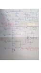
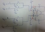
I am designing a circuit which uses a switched capacitor integrator,
The problem is that the desired output is very sensible to the dc offset of the amplifier,
I have been searching for offset-compensated SC integrator topologies....Apparently each compensates more or less offset and has its drawbacks..
One of you has ever tried a certain configuration that proved efficient ?
Does anybody still using integrators without offset cancellation ? Offset cancellation schemes are always taken into consideration ??
Thanks in advance for your answers!!
 

the simplest technique is auto zero. it requires just 1 more capacitor, and a switch. you can also do chopping, or cds. for high performance circuits where the offset can become a signal i usually az, but most of the time the offset is negligible due to the large A0 of the amp itself. (assuming matched parasitics and caps).
 
Ruby, in most cases an integrator is not used as a "stand-alone" circuit but as a part of an overall closed-loop with negative dc feedback (e.g. filters).
In this case, dc offset shouldn`t be a problem.
Therefore, the answer to chrutschow`s question is important: What is the overall function?
 
The integrator configuration is intended for generating a ramp (differential mode), the excursion of the steps of the ramp depend on the ratio between the sampling capacitor and the feedback (or integrating) capacitor...And as i want to generate steps of the order of 100uV, the ratio between the two capacitors should be of the order of 10000 if the difference between the two references that are fed to the sampling capacitors is 1V.......For example, sample in 1 femto capacitor and integrate in 10 pico capacitor....Such a huge ratio is hard to match...so the 1femto capacitor I "virtually" make it by charging 2 capacitors which have a 1 femto difference....Please refer to the attached image to see the two configurations i am talking about....In the first one the offset is no problem because it is multiplied by a ratio of capacitors which is of the order of 1/10000....But in the second configuration the offset is multiplied by "(Cs1+Cs2)/Ci" which is of the order of 1/5, so 10mV offset will generate 2mV steps that will completely "destroy" the desired 100uV steps generated by the ratio "(Cs1-Cs2)/Ci".......I absolutely need to add some offset cancellation scheme.....Which one do you think will be the most appropriate for my design ? please advise,
 

Attachments

  • Ramp_gen.jpeg
    Ramp_gen.jpeg
    552.1 KB · Views: 133

i would first verify you arent creating 'offset'(more like a gain error) by charge dumping by your switches. after you verify those arent a problem, i would ask how much dead time you can tolerate between phase 1 and phase 2. typically an AZ circuit is performed in the nonoverlap of the 2 phases, in your case it would be when all switch 2s are open, you would need two az caps since you are using a fully diff amp. and about 4 az switches. another possible path would be to use your inputs but change the switching configuration to perform a type of ping pong so you do a double integrate for each expected integrate, but make the integrates half value, then integrate the sig alternating between inputs. this will give you a ((Cs1+Cs2)/Ci)*dVref+vos + (Cs1+Cs2)/Ci)*dVref-vos = 2*dVref*((Cs1+Cs2)/Ci) , where Cs1+Cs2/Ci = half your current ratio. This could also help to reduce your insane ratio of 10000 to 5000, allowing your subtracted value to be double the tolerance. or if this is a mass production part, more importantly half the layout space of your Ci(which you have 2,so is like eliminating a full Ci, and at 10pF thats huge savings). But for beginners I would 1st replace the amp with an ideal, and verify that even if the amp itself had 0 mismatch that the sc circuit is accurate enough.
-Pb
 
Prestonee, what you are suggesting seems really interesting but i confess that i did not understand all of it:
There's no charge dumping by the switches,
I can tolerate as much time as needed between phi1 and phi2....You said that an AZ circuit is performed in the nonoverlap of the two phases...then you said it's when all switch 2s are open...in my understanding during the nonoverlap all the switches are closed...can you please recommend me some documents where i can understand the basics of Auto Zero ?
About the other path: From what you said i thought that may be it was not clear in my schematic that the ratio [(Cs1+Cs2)/Ci] is the unwanted one....This ratio is of the order of 2/10...The "insane" ratio of 10000 i make it with the "difference" of Cs1 and Cs2 divided by C1, or [(Cs1-Cs2)/Ci].....In the second configuration the offset gets multiplied by [(Cs1+Cs2)/Ci] which is not negligeable....where does the term [(Cs1-Cs2)/Ci] go in what you are proposing ?
Also, in the equation that you have written: [((Cs1+Cs2)/Ci)*dVref+vos + (Cs1+Cs2)/Ci)*dVref-vos] i can see that there's a "+vos" term and a "-vos" term...the amount of offset that gets sampled at the negative/positive inputs of the amplifier is either positive or negative right ? how can you create -Vos and +Vos in the sampling process so that they conceal each other ?
I am simulating this circuit with an ideal amplifier from mentor's MGC LIB,
 

for AZ you add caps in series to your ota input pair. the nodes connected between your ota pair and the az cap I will call internal inputs, the other node of the caps will be called the external inputs. in AZ mode you need to sample the offset onto these caps, to do this you will be removing your input caps and placing the az caps into your circuit as if they are the input caps. so you open the switches from your input (removing them from the circuit), close switches from the external inputs to cm (shorting inputs to cm) and close the switches between your internal input and your feedback caps( gives you a single sided equiv of integrating your cm, this will capture the difference of inputs on your input cap) You will see that on one side of the az caps you have cm voltage tied(same voltage potential), on other side, the internal input sides, you have isolated nets thats ideally are equal (your high impedance ac ground) these are your input offset sources. at this point you now have the caps sampling your offsets with respect to cm. then when you go to normal operation, you keep the az caps in series with the ota amp inputs, but change the feedback cap from internal input to external input(this puts the inverted az cap voltage in series with your input offset voltages canceling them out. The az references I have in books are for single ended only but you should be able to see how i expanded this to the full diff version i described. This would be Allen and Holberg CMOS Analog Design, just look up Auto Zero in the index.

- - - Updated - - -

I'll anwser the last question before the middle stuff , cause tis easier and less thinking this morning, although offset is a bit of an unknown number until you get silicon, you know it is consistent. It will never change polarity in the use of the circuit, and under the same gain and feedback network it will not change in magnitude. Relying on this you can cancel it out by relying on the symmetry of a fully diff amp. since pos, neg input/output are switchable(as long as you switch the input and the output, you will not notice a difference in signal(except in the non symmetric offset). Thats the premisses of ping ponging the inputs and doing a double integrate. To do this you never do a sample per say, I will simplify this for easier passage of thought. 1st integrate your + input on side P with respect to - input on side N, then change your summing junctions and outs polarities of your amp with respect to the feedback networks (results in flipping the ota within the feedback network). Now that I think of it, I believe this is the common method for chopping.

The above is just a method for flipping the ota to cancel out offset, but you can do the timing 2 different ways. one way is to keep the timing and feedback caps the same across the board and accept you will be adding offset on 1 output and removing it with the next output, so your output steps would be out + vos, out - vos, out+vos, out - vos, etc. this makes your steps have a delta of 2 vos. but average to 0(net integration of vos =0)
If you want your steps to be equal as well as the net int being 0, you need to adjust the timing and the caps. half your input caps and integrate two times faster , and sampling your integrator every two integrates.
I would atm disregard my comments about the equation , I misunderstood something.
1 question though, it sounds like you are using such a tiny ratio because your inputs are so large. have you thought about using something other the cm as a reference? for example using cm + dV for pos reference and cm-dV for neg , where abs(-dv) = dv. this would give you gain reduction without having to use such large caps. (this is typically used in flash converters, for sizing signals).

Thank you for your response Prestonee. I have just downloaded the book by Allen and Holberg...I will study your response and come back to you,
 

Ok Now i understand the auto zero approach thanks.

Can you give me a reference where i can understand the approach of ping ponging the inputs and doing a double integrate ? From your explanation it seems to me that it will be more interesting, you said that it's the common mode for chopping...I have been reading about chopping but i found only explanations about its benefits in the frequency domain...Can you please recommend a reference whre i can find a clear explanation of the double integrate/ping ponging the inputs ?

Yes the difference between my plus and minus references is 1volt....What do you mean exactly by sizing signals in flash converters ? In my knowledge they use resistor or capacitor dividers to obtain various references for comparators....Is resistive voltage divider what you are talking about ? or there is something else i'm not aware of ? any reference please ?
 

the double integrate concept is very simple, 1st make note that a fully differential amp is purely symmetric, in that if you apply a diff sig vin with vinp being on inp of the ota, and measure the voltage and sign of the output, it will be equal to if you flip your input so the vinp is on inn of the ota and measure the output voltage so that vout=outn-outp. once you understand this you can then extend it to say the only non symmetry will be the offset voltage. so if you integrate once, then flip the ota, and integrate again, you will have 2 integrates and a cancelled out offset voltage. this has a side affect of chopping if done at 2x the normal rate.

yes they do that to obtain various references. that is what i am suggesting, if you know your signals are so large instead of attenuating with a large Cf to Cs ratio you could attenuate by subtracting voltage off both(using a reference thats equal to vcm + some offset). however you can only do this as long as the abs(sig) is larger then the offset. example= say refp = 1.4v and refn = 0.4v, your vsig = 1V, you wish this to generate 100uV..you could charge input caps to refp-(cm+.25) and ref-(cm-.25), giving you 1.4-(.9+.25)=.25V and refn=-.25V as opposed to +.5 and -.5V. so you have already attenuated by a factor of 2 before even getting to the cap ratios. but again you can only do this if your signal is always greater then the offset voltage being added/subtracted from cm. if refp was only 1V, then outp= -.15V and outn=+.15V meaning you now have inverted your signal.

hope this helps
-Pb
ps if anyone thinks i said something wrong or misleading feel free to correct
 
Ok now i think i understand the concept of double integrate to eliminate offset...but does this hold for a fully differential amplifier too, which have 2 outputs ?
 

Hello Again!
I implemented the auto zero scheme first using an ideal amplifier.......it worked with the ideal amplifier,
But when i replaced the ideal amplifier with a real one, the obtained results were weird: If i connect the amplifier as follower during the first phase i obtain outputs that oscillate between the common mode and Vdd....and if i keep the feedback capacitor the output starts to integrate than saturates at a certain level.......in the book it is said that only self compensated high-gain amplifiers should be suitable for autozeroing....what does this mean ? how can i know if my amplfier is even suitable for autozeroing ? how should i connect the amplifier during the first phase so that it won't give weird results ? in which cases autozeroing might not be feasable at all ? Thanks!
 

can you screenshot your current az configuration?
its a bit tough to know how you are doing it without seeing it.
thanks
-Pb
 

Prestonne,
Please find attached the schematic i am using for autozero: during phase1 I sample the input capacitors and the auto zero capacitors, and during phase 2 i integrate by connecting the feedback capacitor "after" the auto zero capacitor so that the amplifier's offset is canceled. My question was about whether to keep the integrating capacitor around the amplifier during phase 1 or just connect the amplifier as follower....Anyway, when i used the ideal amplifer from mgc lib it worked both ways...but using a real amplifier did not work....Please advise, thanks,
 

Attachments

  • AZ_ed.jpg
    AZ_ed.jpg
    3 MB · Views: 100

I believe you need to close the feedback first. the reason is because if you connect the inputs in phase 2 before closing the feedback, you are essentially creating a open loop amplifier, meaning you just changed your gain of which is as you stated earlier a small fraction to about 50to 100dB causing instant railing. But looking at your static phase 1 and your static phase 2 they look correct to me(assuming the red penciling phase is part of your phase 2). you might verify the actual timing of your switching, I was taught to use a p1 and a p1q, p2 and a p2q. where the q means quick, or occurs 1st. my 1st comment about closing feedback 1st, i was referring to making the feedback p2 a p2q, and the inputs p2 stay a p2. what is your open loop gain?
-Pb
 
Prestonee, you are right, the problem is apparently with the timing...initially i only made p1 and p2 non-overlapping, and then when i created a p2q and p1q the amplifier started integrating around the common mode but it saturates at a certain level....I made the delay longer to check if it will make things better but doing this crashed the resut completely (the outputs stay around vcm and there is no integration)....So now i believe i just need to fix the timing of the switches, i tried many configurations but here i'm going to ask a few questions to be sure what i am doing is not wrong: the "quick" clocks (p1q with respect to p1 and p2q with respect to p2), they come first on the rising edge or on the falling edge? or on both of them ? how should i place them with respect the the non-overlapping of p1 and p2 ? should they be nonoverlapping, p1q and p2q ?? i don't know if i can just put any delay or taking into consideration the non-overlapping is important...My period is 20ns....what would be the order of the delay ? Please advise,
And btw, the open loop gain is about 70dB i think,
 
the 'quick' clocks are typically created by adding an extra set of inverters between them and the non quicks.
you generate the Qs, then use inverters to make the normals. so by nature they are non overlap, and have the same non overlap as the original. the original clocks will be delayed only a slight amount, enough for the rising and falling to take place. depending on your technology and loading this will vary. I am attaching an example feedback circuit of an auto zeroing integrator I use. This is half of the feedback, the sc circuit on the right is just the cmfb so ignore. autoz.jpg

- - - Updated - - -

and ignore the chop comment, it was disabled in this version of the schematic
 
Ok. Thanks a lot Prestonee for all your answers. I think that the timing of the switches is good now, as well as the az configuration...but i still don't have the result i want and now i understand that i have another problem that i have to deal with (Well on this one i think i will have to fly solo to resolve it): Before implementing the auto zero scheme i used to leave the amplfier sample common mode voltages only until its outputs reach the output common mode voltage and then i connect Vrefp and Vrefm to start integrating.....But now that i have the AZ scheme i have to figure out how to make the amplifier's outputs go until Vcm and stay there until i connect the plus and minus references to start integrating.....Caus now with the presence of offset at opamp input he integrates even if i feed him common mode voltages only and on their way to CM the outputs of the amplifier rail !! The problem with the real amplifier now is dealing with common mode establishment before the beginning of integration....That's why it worked with an ideal amplifer and not with a real one!!! Analog circuit design is such a complicated thing to do!!!! Thanks a lot for your help anyway,
 

Status
Not open for further replies.

Part and Inventory Search

Welcome to EDABoard.com

Sponsor

Back
Top