Continue to Site

Welcome to EDAboard.com

Welcome to our site! EDAboard.com is an international Electronics Discussion Forum focused on EDA software, circuits, schematics, books, theory, papers, asic, pld, 8051, DSP, Network, RF, Analog Design, PCB, Service Manuals... and a whole lot more! To participate you need to register. Registration is free. Click here to register now.

Netlist difference between LVS layout and schematic in Calibre

Status
Not open for further replies.
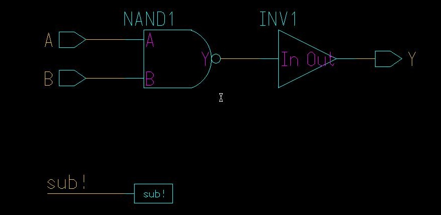
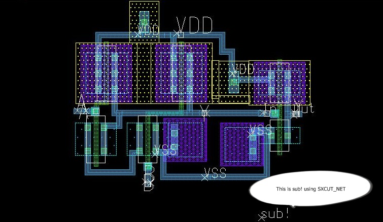
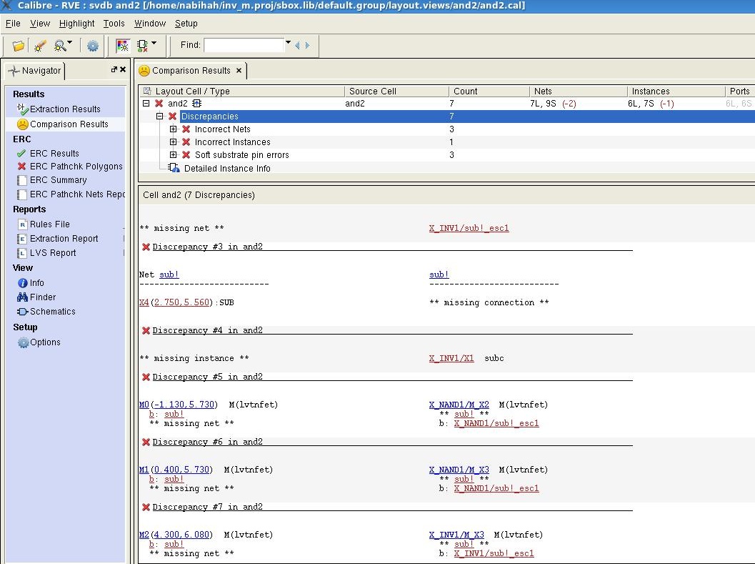
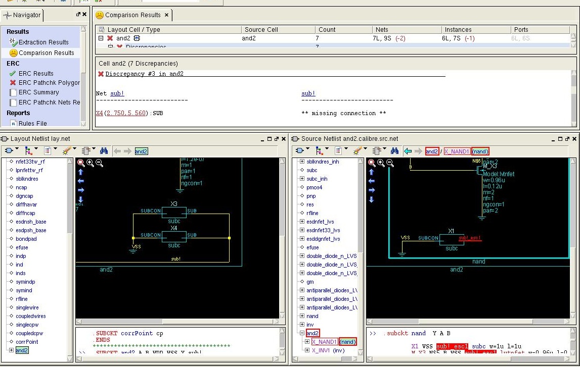
I'm using cmrf8sf V1.7.0.0DM, and based on the layer info, SXCUT_NET is for label purpose.
How I'm gonna add global sub! in schematic, is it with the subc device?sorry if this like dumb question to you..i just want to make sure I'm done it right.
Thanks
 

no I am suggesting that you define in your schematic entry tool (which I assume is not Cadence since having a final ! is sufficient to make a net global) that sub! there is indeed a global net, how did you get VDD and VSS to be netlisted as global? do the same for sub!
 
Last edited:

Hi

I've put global sub! (which I thought the right global) in the schematic, but other error appeared.
See the picture below


I'm so stucked now...please help me..
 

why is the name of the substrate in the schematic cells different? sub!_esc1 instead of sub!?
 

That's confused me too, I don't know how it's happen. My schematic have sub! for each of the cell, not sub!_esc1.
You see here, I think the global sub! I add is fine in the layout, but it cause badly to the schematic


you do not seem to have this problem on VDD and VSS what is different between those nets and sub! ?
 

It is because for VDD and VSS I've used global VDD and VSS device from the library.but for the global sub! I've found one global device from the library and used it, because when I've checked the property it is global, just changed the value to sub!.
I don't have other any idea how to make global sub! than this way.
 

is this global device used in both INV and NAND cell?do those cells have their own layout? in that case are they LVS clean?
 

It is because for VDD and VSS I've used global VDD and VSS device from the library.but for the global sub! I've found one global device from the library and used it, because when I've checked the property it is global, just changed the value to sub!.I don't have other any idea how to make global sub! than this way.

I think that things are becoming more complicated...
What do you mean with this?
I've found one global device from the library and used it
I suppose that this global device is subc.Is this true or not?
In any case,if it is from a library then you should better not change things that are default.Stay and live with them if you want less or no trouble ;-)

dgnani gave a good contribution.Is each individual cell (inv,nand) with it's own subc LVS clean?
If yes then the problem is located to the interface of those two cells.

Additionaly,in this image https://obrazki.elektroda.pl/12_1314225641.jpg you uploaded i see a subc in the top level schematic.This is not needed there,since there are not devices in the top-level design that need connection to substrate.Remove it.

Another idea is to create a simple a test case to see what is going on...one transistor and one subc.Nothing else.Is this LVS clean?
Ofcourse don't change any parameter of subc.

If you don't mind,what tool do you use for your design?The above images don't seem to be extracted from Cadence environment...
 

I think that things are becoming more complicated...
What do you mean with this?
I suppose that this global device is subc.Is this true or not?

This is global device in image in the top level schematic. For each cell I've used subc device which is the property is subc, not Global like VDD and VSS.


Is each individual cell (inv,nand) with it's own subc LVS clean?
If yes then the problem is located to the interface of those two cells.

Each individual cell have a LVS clean, the LVS problem only happen when I've used it together to form a top level layout.

Additionaly,in this image https://obrazki.elektroda.pl/12_1314225641.jpg you uploaded i see a subc in the top level schematic.This is not needed there,since there are not devices in the top-level design that need connection to substrate.Remove it.
I thought this is the way to put global subc as you have suggest before, which I've need to add subc to the top level schematic.

Another idea is to create a simple a test case to see what is going on...one transistor and one subc.Nothing else.Is this LVS clean?
Ofcourse don't change any parameter of subc.
I don't understand this, this is like doing INV design, isn't, as I told you, my INV and NAND gate have LVS clean

If you don't mind,what tool do you use for your design?The above images don't seem to be extracted from Cadence environment...
I've used Calibre with mentor graphic tool (Design Architect and IC station)
 

I have never used IC Station so you need to read the schematic tool manual to see how to define a global nets (as far as I understand you need the 'global' or 'vee' cell form the MGC_IC_GENERIC_LIB library)

If you cannot figure out how to get the global to work then you can always bring the sub! net to an explicit terminal and use it that way, ugly but it will let you move on
 

I have never used IC Station so you need to read the schematic tool manual to see how to define a global nets (as far as I understand you need the 'global' or 'vee' cell form the MGC_IC_GENERIC_LIB library)
I will have a look on this one..

If you cannot figure out how to get the global to work then you can always bring the sub! net to an explicit terminal and use it that way, ugly but it will let you move on
Can you explain how to do it this way?what do you mean by always bring the sub! net to an explicit terminal?

Thanks
 

Ok...let's put some things in some order.

Since each independent cell is LVS clean the problem is definetely in the top-level.Additionally forget SXCUT since you can pass a clean LVS for the two separate cells.
I insist to remove the subc device from top-level schematic and layout as well,it is definetely wrong!It's existence has no meaning there! (Why?I explained in my previous post).

Now,the problem must be reduced to the interconnection of the two sub! nets of each individual cell you have.
If each subc network in each cell's layout goes to the VSS line of the respective cell and then you connect the two VSS lines to one final (top-level) VSS then you should be correct to clean up LVS.
If you ensure that the above line i wrote is true for your layout then you must turn to IBM's support team to ask for further help sending your case and describing the problem.
They can reproduce the results and propose you a solution.
 

For those who are working in ic station, you can add substrate contact to your pmos and nmos from DLA devices>Guard>path GB>(Psub or nwell) and add them to nets VDD and VSS (click the psub or nwell and connectivity>nets>add to net>chosse VDD or VSS accordingly).
 

Status
Not open for further replies.

Part and Inventory Search

Welcome to EDABoard.com

Sponsor

Back
Top