Continue to Site

Welcome to EDAboard.com

Welcome to our site! EDAboard.com is an international Electronics Discussion Forum focused on EDA software, circuits, schematics, books, theory, papers, asic, pld, 8051, DSP, Network, RF, Analog Design, PCB, Service Manuals... and a whole lot more! To participate you need to register. Registration is free. Click here to register now.

[SOLVED] negative feedback operational amplifier

Status
Not open for further replies.

Junus2012

Advanced Member level 5
Joined
Jan 9, 2012
Messages
1,552
Helped
47
Reputation
98
Reaction score
53
Trophy points
1,328
Location
Italy
Activity points
15,235
Basic question

for the inverting op-amp connection shown. how the op-amp assures that the input viltage difference between its terminals are zero when we apply the negative feedback. I know the Op-amp should have very high gain but still i need a reason to explain why not the inverting terminal can have a different value from the non inverting at the time when we are changing the input signal ?? .

6085902400_1350857906.jpg


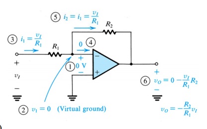
The question is also valid for another negative feedback configurations

Thank you all :)
 
Last edited:

i2=(0-vo)/r2

The opamp TRIES to force the voltage at the inverting input to equal the non-inverting input. In reality there actually is a finite difference between the two inputs.
 

I think you are right senan... If the input voltage could be changed by a relatively fast step, there will be an overshoot (likely damped one) at the output due of the opamp internal delay from input to output before the output is settled at its end value. So during the overshoot, the difference between the two input terminals is not close to zero.
 
I think you are right senan... If the input voltage could be changed by a relatively fast step, there will be an overshoot (likely damped one) at the output due of the opamp internal delay from input to output before the output is settled at its end value. So during the overshoot, the difference between the two input terminals is not close to zero.

Kerim, at first: Nice to hear from you (because the trouble in your country).

I believe the question from Senan is a general one - that means: He is not referring to a step response.
Of course, Barry is right in saying the opamp would "try" to equalize both voltages at the input terminals. However, this is not always understood resp. accepted by beginners.

Senan - you must try to understand the concept of negative feedback.
Perhaps it helps to start with the role of the emitter resistor RE in a common collector transistor stage (voltage follower).
The voltage developed across RE follows the input signal voltage which means: The differential base-emitter voltage remains very small (in comparison to the signal input).
And - the higher the transconductance gm (proportional to Ic) the smaller this diff. voltage.
Something similar happens in an opamp with negative feedback, but due to the very high gain we can count with a differential voltage of 0 volts between both input terminals (in reality: some µVolts).
 
Thank you all for your participation
I usually know that because of the negative feedback and the high gain this will lead to approximately zero difference voltage between the op-amp terminal but i am unable to the mechanism of it for example for the circuit I have shown, so please could you explain this to me. for the voltage follower (buffer connection op-amp) it is very easy to believe that as all the output will be back to the input making the two terminals equal, but in the non inverting or inverting we are feeding back a portion of the output signal not all

Looking again to your answers
 

Senan,

looking at the formulas in wikipedia

https://en.wikipedia.org/wiki/Negative_feedback_amplifier

you arrive at a voltage at the inverting terminal that is

Vin- = Vin/(1+beta*Aol).

Therefore, for beta=0.1 and a standard opamp (Aol=1E5) we arrive at Vin-=Vin/1E4.

Thus, it is not 100% correct to calculate the resistor values under the assumption Vin-=0. However, the calculation is simplified and the error is small enough to be acceptable in comparison to other errors (parts tolerances, parasitics).
On the other hand, this formula gives you an impression on the minimum acceptable product beta*Aol (loop gain) for each specific application.
Of course, there are cases where you have to take into account that the input voltage Vin- has a finite value (falling loop gain).
 
You can try to replace the opamp with its ideal model, i.e. a voltage-controlled voltage source at the output controlled by the differential input voltage (Rin is assumed to be infinite and Ro zero). From this equivalent circuit you can calculate the gain as -(R2/R1)/(1+(1+R2/R1)/A), which goes to -R2/R1 when A goes to infinity (so far the sedra-smith analysis). This means that, for a finite input voltage vin, the output voltage must also be finite (because vout= -R2/R1 * vin). For the output voltage to be finite you require a zero differential opamp input, which justifies the effective short at the opamp's inputs (also sedra-smith analysis).
 
Status
Not open for further replies.

Part and Inventory Search

Welcome to EDABoard.com

Sponsor

Back
Top