Continue to Site

Welcome to EDAboard.com

Welcome to our site! EDAboard.com is an international Electronics Discussion Forum focused on EDA software, circuits, schematics, books, theory, papers, asic, pld, 8051, DSP, Network, RF, Analog Design, PCB, Service Manuals... and a whole lot more! To participate you need to register. Registration is free. Click here to register now.

Need your help on a Band Gap reference design !

Status
Not open for further replies.

fanrong

Banned
Joined
Oct 20, 2006
Messages
122
Helped
3
Reputation
6
Reaction score
1
Trophy points
1,298
Activity points
0
97_1167528522.GIF


Hi , everyone :
I have some quesition on the bandgap reference design :
1. In Gray's book , it gives the equation below :
Vbdg = Vgo + Vto(γ-×)
and Vgo=1.205 , γ=3.2 ,×=1 .
so , Vbdg=1.262 @300k
And Vgo = Eg/q , and is 1.12@300k and 1.205 @0 k , so we can get Vgo
from the transistor's model file . My question is ,how to get the value of ×,γ
from the transistor model file . I do several simulation with different bipolar
transistor model , they all give the result about 1.1 V , but 1.2 .
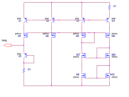
2. In the attached figure , M8 and M10 's W/L is 30/2 , but M7 is 30/4, M9
is 30/1.5 . Does this help to decrease the minimum power supply voltage?
3. I set @300k the TC=0 . I did the temperature sweep from -40 to 180 ,
below 400k , the curve is just like any non - curvature corrected bandgap
reference , but above 400k , the Vbdg begin increase . So how is happened ?
 

Would anyone do me any favor on my questions ?
 

what 's the reason of no people response ?
 

Am i not understanding this right or is the base of the pnp is floating?
 

different models have differnet Vgo.

at high temperature, maybe, the model of BJT and mos are not accurate.
 

Assuming you diode connect the pnp,
1. I think the parameters y and x are not all process parameters. one of them I think is a circuit parameter that relates to the current going into Q5.
2. Imbalancing M7 and M9 will cause a VDS mismatch between M8 and M10 that can cause an error in the current generated. However, you can probably gain some voltage headroom if you reduce the length of M9. So, there is a tradeoff.
 

I'm sorry , Q2 should be diode connected .
But I did not get my answers yet .
Acording to Gary 's textbook , Vref = Vg0 + (alfa - gamma) Vt ,
my question is Vg0, how to get alfa, gamma from the spice model .
 

This would be my suggestion/comments:

Alfa to my understanding is the TC of the current source that goes into Q5 (also mentioned in Gray's book), and thus am finding it hard to see how I would be able to find alfa in a spice model, which contains process parameters.

Gamma, on the other hand, like you say is a process parameter and "could" be found in spice model. However, gamma is related to the temperature dependence of the electron mobility (un). (un is proportional to T^-n) and
Gamma = 4 - n.
I would probably keep track of the mobility (MUS, BSIM model name) w.r.t temperature and back calculate what n is and thus find Gamma.

I dont know if this helps but at the very least lets hope it gives you a starting point.
 

Vbdg = Vgo + Vto(γ-×)
and Vgo=1.205 , γ=3.2 ,×=1

×=1 (in your circuit, this parameter is 1, as your VBDG setup PNP is biased by PTAT current)

γ=3.2 (look inside pspice model for XTI)

Vgo (pspice uses EG, the fictitious Vbe at 0K, not quite measurable in practice)

if u have done an almost ideal job on your bandgap circuit, the 0TC bandgap voltage simualted should be that predicted by the equation. However, u r going to get screwed by your beta and beta's TC. Also playing some part would be the parasitics RB, RE. Think hard enough to reduce your circuit's dependence on beta. p/s: Depending on the fab's ability to control beta, u may not need to compensate it afterall.
 

Status
Not open for further replies.

Similar threads

Part and Inventory Search

Welcome to EDABoard.com

Sponsor

Back
Top