Continue to Site

Welcome to EDAboard.com

Welcome to our site! EDAboard.com is an international Electronics Discussion Forum focused on EDA software, circuits, schematics, books, theory, papers, asic, pld, 8051, DSP, Network, RF, Analog Design, PCB, Service Manuals... and a whole lot more! To participate you need to register. Registration is free. Click here to register now.

Multiple Feedback Filter Not Working as Expected

Status
Not open for further replies.

tomk

Newbie level 6
Joined
Oct 15, 2012
Messages
14
Helped
0
Reputation
0
Reaction score
0
Trophy points
1,281
Activity points
1,431
Hi,

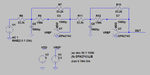
I've got a circuit that consists of two identical low-pass multiple feedback filters in series, and I'm getting almost no attenuation through the second stage. The cutoff frequency is 1 KHz, and the signal that I'm putting through the filter has a component close to DC and a component at 25 KHz, which is what I'm trying to filter out. I get a lot of attenuation at 25 KHz through the first stage, but if I compare the signal out of the first stage with the signal after the second stage, they are almost identical.

Some other notes:
- The GBW product of the opamp is 7 MHz.
- If I replace the second stage with a simple RC with a cutoff of 1 KHz, the 25 KHz component is almost completely removed.
- I used **broken link removed** to choose part values for the discrete components.

Any thoughts on why I'm not getting any attenuation through the second stage would be a big help.

Thank you.
 

One other piece of info: I simulated this circuit using LTSpice, including the model for the opamp in the circuit. No problems found in the sim.

Any ideas?

Thanks!
 

One other piece of info: I simulated this circuit using LTSpice, including the model for the opamp in the circuit. No problems found in the sim.
Any ideas?
Thanks!

If only one of two identical stages works as expected there is only one explanation: hardware failure.
 

Thanks for the suggestions. I had the same thoughts, so I'm glad to hear I haven't done something obviously dumb/crazy.

There are three identical channels on the pcb, each with the two stage filter, and they all have the same behavior, so parts failure is unlikely. I also "beeped" out the whole circuit with a multimeter, so I'm pretty sure it's wired correctly.

I've got another board already built up, so I'll check that one to see if does the same thing.

In the meantime, any other ideas?

Thanks again.
 

Are you possibly using a dual OP? In this case you should pay attention to the channel crosstalk specificationin in the datasheet. It may be simply too poor to allow the intended attenuation. Besides specified "real world parameters" there are many ways to parasitic circuit properties (e.g. capacitive coupling, insufficient supply rejection) to work the same way. Also ground impedance may be a problem.

In any case you should measure the tranmission characteristic of the second stage on it's own to verify that it's working at all. And post a schematic to allow a qualified discussion.
 

Two questions:
*Are you working with single supply ?
*What is the dc gain (R3/R1)?

Hi Tomk,

in addition to the two questions above a third question just came into my mind:

Independent on the problems you have described I like to ask you if both 2nd order stages really are "identical" (as you have written).
Have you designed both stages independent on each other? I don`t know if you are aware that this is not the classical way to design a 4th order lowpass .

Example: A 4th order Butterworth filter consists of two different 2nd order stages none of which has a Butterworth characteristic.
 
  • Like
Reactions: FvM

    FvM

    Points: 2
    Helpful Answer Positive Rating
Thanks for all the comments/questions. Sorry to say that I haven't had a chance to do any debugging on the circuit, but just wanted to address your questions.

- A schematic is attached.
- There is a single 5V supply.
- The DC gain of each stage is -1.
- I am using a dual opamp (OPA2743).
- I suspected that this is not the classical way of doing a 4th order filter, but I would expect better results than what I'm seeing. For next time, do you have a suggestion for a good reference on active filter design?

Thanks, and I'll try to get some debugging in today. For now, I just tacked on an extra RC filter to the output, which makes the circuit usable for my immediate needs, but I'd like to figure out what is wrong so I can avoid the problem next time.
 

Attachments

  • mfb.png
    mfb.png
    25.4 KB · Views: 77

A second order filter with cutoff frequency 1 Khz and unity gain at dc (like your stages) attenuates roughly 25*25 times at 25 KHz, i.e. 56 dB. So you should be measuring weak signals.
Spurious paths in the measurement setup, grounding effects, parasitic couplings, etc., can be relevant. It is important to see how are you mesuring the signals. How is it?

Regards

Z
 

Hi tomk,

the problem is - as I have already expected - the single supply operation.
Explanation: With Vref=2.5 volts and a non-inverting dc gain of Gdc=+2 the output of the 1st opamp has a dc potenial of (nearly) +5V.
Thus, the problem is the FIRST stage. The problem can be solved by using a large input coupling capacitor, which reduces the dc gain to Gdc=+1.
Do the same for the 2nd stage also.
 
To design a proper 4th order filter with better rolloff then the two second-order filters you have, you can use the FilterPro program which is a free download from Texas Instrument.
 

To design a proper 4th order filter with better rolloff then the two second-order filters you have, you can use the FilterPro program which is a free download from Texas Instrument.

I think you will agree that the roll-off of EACH 4th order filter is 80dB/dec.
The difference between a series connection of two equal 2nd order stages and a "proper" 4th order filter primarily is in the transition area between the pass band and the stop band region.
 
LvW, I don't understand your note about the single supply. Would you mind explaining a bit more? Are you saying that I'm railing the opamp on the first stage? I must be misinterpreting what you mean by non-inverting DC gain, because I would say that it is Gdc=+1 (R7/R8 in the schematic I posted) and not +2 as you suggested. To be clear, the signal that I'm filtering is centered at 2.5V, which is why Vref=2.5V. If the input signal (DC level + ripple) exceeds 0-5V, then I would understand why the first opamp would be at a rail, but otherwise I don't see it.

Also, for the large input coupling capacitor, could you be more specific about where it should go? From the left side of R8 to ground?

Thank you for the FilterPro suggestion. I'll check it out for next time. In this application, I don't care too much about the behavior in the transition between pass and stop bands (within reason). I just need to have a lot of attenuation in the stop band, so I think I'll be ok with this topology. Maybe this is covered in another thread, but does anyone have any favorite books on this subject?

Thank you all for your help. Much appreciated.
 

Without a capacitor on the input, the non-inverting gain from the 2.5V reference is 2 (1+ R7/R8). That's why you need a DC block capacitor in series with the input. That effectively makes R8 equal to infinity at DC and the non-inverting gain becomes 1, as you intended.
 
  • Like
Reactions: tomk

    tomk

    Points: 2
    Helpful Answer Positive Rating
Yes, crutschow gave the correct explanation already.
Nevertheless, some more details:
* You have two input signals for the 1st stage: 2.5volts dc at the non-inv. input and the ac signal to be filtered at the left side of R8 (without a coupling capacitor).
* But both are differently amplified: The dc value with the non-inv. gain of Gdc=1+R7/R8=+2 and the input signal (as desired) with the transfer function H(s).
* Thus, you have at the output of the 1st opamp the superposition of two signals (dc and ac). And the dc value is Vout=2.5*2=5 volts, which means that there is no "room" for any ac output signal.
* You must try to provide the output with a dc value (that is the operating point of the 1st stage) just at Vcc/2.
*That means: the dc gain of the stage must be reduced to unity. This is accomplished by increasing the dc value of the first series element (R8) to infinity - without disturbing the filter function (which needs R8).
* Solution: A large input coupling capacitor Cin, which does not influence the filtering properties of the circuit (Cin as large as possible).

Any further question?
 
  • Like
Reactions: tomk

    tomk

    Points: 2
    Helpful Answer Positive Rating
The LTSpice simulation schematic has a sine source with offset, SINE(2.5 1 25k) means 2.5 V offset 1V amplitude, 25 kHz. This means, at least in the simulation there's no biasing problem. But I don't know how the input signals looks like in the real circuit.

I assume, that you have checked the DC level? How did you check the filter operation?
 

Ok, now I see what you're saying and it makes sense. The only problem is that I need to retain the DC component of the input signal, so I don't want to remove it with a big input cap. The input signal is a DC component plus ripple at 25KHz. The intended purpose of this filter is to remove the 25KHz ripple, but retain the DC signal (centered at 2.5V). For example, if the input is 3Vdc + 1V@25KHz, I want the output from the first stage to be 2Vdc and nothing at 25 KHz.

It mostly works, meaning that on the output of the first stage I see a DC signal that is the same as the input, inverted around 2.5V, plus a small component of the 25KHz ripple. The problem is that I'm not getting as much attenuation of the 25KHz ripple as I would expect on the first stage, and almost no attenuation on the second stage. Is that a result of the DC gain of +2 on the noninverting input?

Is there any way of achieving my goal using the multiple feedback topology. To be clear, the goal is to retain the DC component of the signal, squash the 25KHz ripple, and keep the output centered at 2.5V (polarity doesn't matter).

Thank you.
 

Ok, now I see what you're saying and it makes sense. The only problem is that I need to retain the DC component of the input signal, so I don't want to remove it with a big input cap. The input signal is a DC component plus ripple at 25KHz. The intended purpose of this filter is to remove the 25KHz ripple, but retain the DC signal (centered at 2.5V). For example, if the input is 3Vdc + 1V@25KHz, I want the output from the first stage to be 2Vdc and nothing at 25 KHz.

Tomk, are you aware that it is the first time you mention the dc part of the input signal? This completely changes the situation.
The diagram in your post post#10 shows an ac input only.
Please note: A detailed and helpful answer requires a detailed description of the problem.
 

Status
Not open for further replies.

Part and Inventory Search

Welcome to EDABoard.com

Sponsor

Back
Top