Continue to Site

Welcome to EDAboard.com

Welcome to our site! EDAboard.com is an international Electronics Discussion Forum focused on EDA software, circuits, schematics, books, theory, papers, asic, pld, 8051, DSP, Network, RF, Analog Design, PCB, Service Manuals... and a whole lot more! To participate you need to register. Registration is free. Click here to register now.

multi voltage power supply

Status
Not open for further replies.
Hi,

your trace width is too small. There is relatively high current. And the current is pulsed.

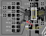
A parameter how much EMI is sent out by your circuit is the diameter of the HF-current-path-
The yellow line shows the currrent path at the time when the switch inside the converter Ic is switched ON.
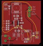
HF-I-path.JPG
With your PCB layout the current has to travel almost around the complete PCB.
But it should be short and low impedance.
-> Use wider tracks and change your placement, so the way is short.

There are two paths for each converter channel. (in your circuit a total of four)
* HF path when switch closes (shown)
* HF path when switch opens = across diode

Klaus
 

- - - Updated - - -

Hi,

your trace width is too small. There is relatively high current. And the current is pulsed.
I will fix this and increase the nettrace width .

A parameter how much EMI is sent out by your circuit is the diameter of the HF-current-path-
The yellow line shows the currrent path at the time when the switch inside the converter Ic is switched ON.
View attachment 123835
With your PCB layout the current has to travel almost around the complete PCB.
But it should be short and low impedance.
-> Use wider tracks and change your placement, so the way is short.

I am not understanding this , how can I make the current path short ? can you suggest a component layout which will achieve this?

There are two paths for each converter channel. (in your circuit a total of four)
* HF path when switch closes (shown)
* HF path when switch opens = across diode

Klaus

I didnt get this either please explain what is HF path ?

- - - Updated - - -

Hi,

There is a very important thing : You need RFB2 like the Original Schematic. The Node between Lower Pin of RFB1, Higher Pin Of RFB2 and FB2 Pin IS NOT GND. In the original schematic , lower end of RFB1 Crossed Over GND Node to RFB2. It's not connected to GND. if it was connected to GND , there was a Junction (those CIRCLES) Like the one between RFB1,RFB2 and the track to FB2 PIN. If you use it like this , your circuit won't work and i think your REG2 Output will be around input voltage.

Also i think it's better that you change RC1,CC1 & RC2,CC2 placement like the evaluation board , in series , not like a loop. (your electrical connection is correct , but you placement seems like a loop, this shouldn't be like this)

P.S : Hope it's not too late (and hopefully you didn't order your PCB ), It seems we live in different time zones.

Good Luck!

oh thats dumb of me .. yes you are right i will redo the circuit and board this evening and show it to you.
I am in east florida .

regards

- - - Updated - - -

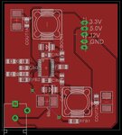
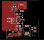
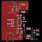
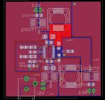
based on Mimarian's correction i fixed the circuit and board layout .
I still have to figure out what Klaus is pointing out , I need help .
LM2717_schematics.jpg
LM2717_board_layout.jpg
 

- - - Updated - - -


I will fix this and increase the nettrace width .


I am not understanding this , how can I make the current path short ? can you suggest a component layout which will achieve this?


I didnt get this either please explain what is HF path ?

- - - Updated - - -


oh thats dumb of me .. yes you are right i will redo the circuit and board this evening and show it to you.
I am in east florida .

regards

- - - Updated - - -

based on Mimarian's correction i fixed the circuit and board layout .
I still have to figure out what Klaus is pointing out , I need help .
View attachment 123866
View attachment 123867

Hi,

Your schematic seems to be OK now.

About other problem : i will do a simple comparison between your board and evaluation board, this should be helpful.

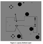
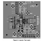
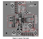
In your board, there is a large ground plane around the board (on Both TOP & Bottom ,i think) and all of it is connected to one Ground Node, GND. In Evaluation board there is 2 Ground Nodes. One is PGND and one is AGND. on TOP layer you see split planes , one is for AGND , one is for PGND , One for Vinput , one for Vout1 and one for Vout2. In Bottom layer there 2 split planes , one for AGND and One for PGND.

if you check the evaluation board carefully , you'll see all of Ground Planes (2 ANGDs & 2 PGNDs on TOP and Bottom) connect together just under LM2717 at 1 point only (star configuration). in this case when the load of REG1 or REG2 changes, it won't affect the other regulator. there is only one way of current flow possible for each regulator.

But in your PCB, because all of unused pcb is GND , You may see a problem because of Ground Loops. In that case, there many way of current flow possible (at least 2 like the one klausT mentioned), and there will make problems. Your pcb will work , but you will see more voltage Ripple than what you expected, EMI problem like what KlausT Said,..etc.

I recommend to study the Evaluation board PCB carefully and apply the changes to your pcb for better results.
 

hi memarian !

i see the various ground planes you mentioned , I also see that the PGND and Vin GND planes are both passing under the LM2717 , but I am confused about the following:

-where is AGND ?
- how are the planes being joined under the LM7217 ?
- I dont see VOUT2 plane connecting anywhere.

can you point out the above on the layout please ?
EVA-BOARD_BOT.jpg
EVA-BOARD_TOP.jpg
 

Thanks d123 I am reading the docs you posted.
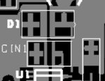
I am analyzing the the TI App note and the schematics show CIN1 should be connected to the PGND but on layout it doesn't seem to be. the + does not seem to touch the ground plane as it does for the D1.
CIN1.JPG

- - - Updated - - -

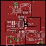
please look at the schematics and board layout , I think I am getting it slowly.
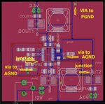
I have some confusions in AGND n PGND which I am posting in the image if someone can clear that out .
thanks
AGND.JPG
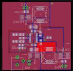
LM2717_schematics-NEW.jpg
LM2717_BOAR_LAYOUT_NEW.jpg
 

Hello again,

Please Check the attached Picture.

EVA-BOARD_TOP.jpg


1) I identified AGND Plane on TOP Layer (same goes for Bottom layer too)
2) After checking the layout again , it seems there is 2 Points that AGND & PGND connect together , I draw a Circle around each one: P1 & P2
3) Vout2 Plane doesn't connect to any thing, it is as Vout2 output to connect to load. you see RL1 & RL2 in Layout,not in schematic , these are dummy loads for REG1 & REG2, which you should connect to your Load.
4) About the problem around CIN1 : i think it's because in those pictures , there is no identification about Via Holes in pictures. I didn't check TI site for Gerber files (sometimes they make EV-Boards gerber files available online), you can only be sure about that with gerber files or other PCB Files.

5) i think you are going in right direction. just take a look at the attached image, and a bit more modification about your PGND/AGND Node.

Good luck!
 

Hi,

here again.
I see others gave good advice.

To your PCB.
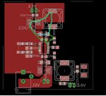
HF-I-path2.JPG
That´s the way to go. See the area enclosed of my green line. It maybe is only 10% than before.
Very nice is the placemenct of the two capacitors next to the output connector. Well done. With this i expect low ripple voltage at the output and low EMI.

Try to go the same way at the other channel. It is more difficult because of the power supply connector and the wires. The try to cut your GND plane into pieces.

To my shown lines: The green line shows the high frequency current path when the switch closes. The cyan one shows the path when the switch opens. Imagine the lines act like a transmitting antenna. The larger the enclosed area, the more EMI is sent out. And also, the more they differ, the more EMI is sent out..because they are acting like two alternating antannes.

Hope this helps.
 

I have added one of the AGND plane please check if it looks ok , i have connected it to the AGND pins on the LM2717 namely 3, 9,10 and I have connected the PGND plane to the 1,2,11,12 pins.

LM2717_board_layout.jpg
LM2717_BLOWUP.jpg
 

Hi,

I´d place the AGND DGND connection directely at the pins.

How did you draw it?
With EAGLE you need just draw the complete GND polygon. Then draw lines in the "top restrict" layer for the cut.

Your PCB is only one sided.. is it possible to create a two sided. It makes electrical things easier.

Klaus
 

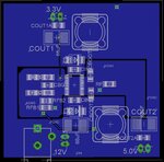
please review the completed schematics and board. I have used few vias to connect the ground planes from top to bottom.

thanks
LM2717_BOARD_TOP.jpg
LM2717_BOARD_BOT.jpg
lm2717_board.jpg
LM2717_schematics-NEW.jpg

- - - Updated - - -

also including the ground and other planes showing isolation .
LM2717_GND_PLANES.jpg
LM2717_VIN.jpg
lm2717_5v.jpg
LM_2717_3.3V.jpg
LM2717_BOOT1.jpg
LM2717_BOOT2.jpg
 

Hello,

With a quick look, it seems everything is OK.

Good Luck!
 

I got two of these boards made , I was using one fine until today it suddenly stopped working , I am not getting either 3.3v or 5v outputs.
I took the second board out and as soon as I plugged the 12v adapter the 68uF caught fire .

what could be causing this circuit to fail and what can I do to prevent ?
I am attaching the parts list which I used for the boards are their any under rated component I used ?

partslist.jpg
 

Hi,

Measure the output voltage of your 12V adapter.

Klaus
 

Hi,

Measure the output voltage of your 12V adapter.

Klaus

oh I thought it was 12v but its actually 15.79 but still this circuit should handle this voltage or not?
 

Hi,

Correct, it should be able to handle 15.79V DC voltage. But is it stable? Maybe it moves from 12V...20++ V.

It all sounds that simple, but there always is a pitfall in the detail.

Klaus
 

I took the second board out and as soon as I plugged the 12v adapter the 68uF caught fire .

what could be causing this circuit to fail and what can I do to prevent ?

View attachment 126967

I have a lot of gray hairs, and many of those gray hairs have been caused by Tantalum capacitor fires.
The company I used to work for invested tens of thousands of dollars and many months performing investigations.


I'm going to make a long story short. When used with a low impedance source, the voltage rating for Tantalum capacitors must be significantly derated. By a lot of margin.
My personal advice, based on my experience, is to use a capacitor rating with twice the operating voltage. In your case, that would mean a 30 volt capacitor.
See the following presentation. Read it from beginning to end.

http://dkc1.digikey.com/us/en/TOD/Kemet/tantalumcapacitors/tantalumcapacitor.html
 

double the power supply voltage would mean I need capacitor of above 30v rating , on digikey these caps are being sold for 6 bucks a piece . I have 3 of them on this power supply , this will make it too expensive.
is there a cheap source for high voltage capacitors ?


Status
Not open for further replies.

Similar threads

Part and Inventory Search

Welcome to EDABoard.com

Sponsor

Back
Top