kissmoh
Junior Member level 1
- Joined
- Jan 17, 2013
- Messages
- 16
- Helped
- 0
- Reputation
- 0
- Reaction score
- 0
- Trophy points
- 1,281
- Activity points
- 1,443
hi im trying to connect each module using 2d wires
for example,
when i use modelism, (im using se 6.5ver.) the signal value('write_px_data[0],...') changed to 'x', suddenly without any trigger value( the output of each module were register) and the problem was solved by changing the name of 2d wires to 'write_px_data_0'.
cannot the modelsim treat the 2d wire connection? can it be allowed in ISE tool?
i want to know the reason.
when i saw the RTL sheme in ISE, the circuit didnt have any problem. then, is it just a problem of modelsim?
The operation of module 'Write_stage' and wiring are perfect
(sry for my poor english skill i hope that it was enough to tell u what i intended.)
///// i attached the original code
and this is the simulation result, the value changed to 'x' suddenly, as stated in below my comments, if i change the name of wire which is connected to this wire(or output port) outside of this module from a[0] to a_0 (not in this module), then the problem disappeared.
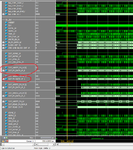
is that a problem if i use 2d wire connection continuously? (i.e. module a output - 2d wire - output port(upper level module of a) - 2d wire ....
for example,
Code Verilog - [expand] 1 2 3 4 5 6 7 8 9 10 11 12 13 14 15 16 17 18 19 20 21 22 23 24 25 26 27 28 29 30 31 32 33 34 35 36 37 38 39 40 41 42 43 44 45 46 47 48 49 50 51 52 53 54 55 56 57 58 59 60 61 62 63 64 65 66 67 68 69 70 71 72 73 74 75 76 77 78 79 80 81 82 83 84 85 86 87 88 89 90 91 92 93 94 95 96 97 98 99 100 101 102 103 104 105 106 107 108 109 110 111 112 113 114 115 116 117 118 119 120 121 122 123 124 125 126 127 128 129 130 131 132 133 134 135 136 137 138 139 140 141 142 143 module en_sig_distributor( //1st stage output OUT_VSYNC_W, output OUT_HSYNC_W, output OUT_DVAL_W, output OUT_ORI_DVAL_W, output [3:0] OUT_PX_DATA_W_0, output [3:0] OUT_PX_DATA_W_1, output [3:0] OUT_PX_DATA_W_2, output [3:0] OUT_PX_DATA_W_3, output [3:0] OUT_WRITE_EN_W, //2nd stage output OUT_VSYNC_R, output OUT_HSYNC_R, output OUT_DVAL_R, output OUT_ORI_DVAL_R, output OUT_READ_EN_SUM_R, output [3:0] OUT_READ_EN_R, /////////////////////////// input nRESET, input CLK, //1st stage input VSYNC_W, input HSYNC_W, input DVAL_W, input ORI_DVAL_W, input [11:0] BLOCK_CNT_W, // 0~2213, 6x6 block, (324*246)/36 input [5:0] ONE_LINE_BLOCK_CNT_W, // 0~53 324/6 input [3:0] IN_PX_DATA_W, input WRITE_EN_W, //2nd stage input VSYNC_R, input HSYNC_R, input DVAL_R, input ORI_DVAL_R, input READ_EN_R ); //======================================== //======================================== wire write_vsync, write_hsync, write_dval, write_ori_dval; // wire [3:0] write_px_data_0, write_px_data_1, write_px_data_2, write_px_data_3; // no problem occured wire [3:0] write_px_data[3:0]; // problem occured wire [3:0] we; wire read_vsync, read_hsync, read_dval, read_ori_dval; wire sum_re; wire [3:0] re; //======================================== //1st stage assign OUT_VSYNC_W = write_vsync; assign OUT_HSYNC_W = write_hsync; assign OUT_DVAL_W = write_dval; assign OUT_ORI_DVAL_W = write_ori_dval; // assign OUT_PX_DATA_W_0 = write_px_data_0; // assign OUT_PX_DATA_W_1 = write_px_data_1; // assign OUT_PX_DATA_W_2 = write_px_data_2; // assign OUT_PX_DATA_W_3 = write_px_data_3; assign OUT_PX_DATA_W_0 = write_px_data[0]; assign OUT_PX_DATA_W_1 = write_px_data[1]; assign OUT_PX_DATA_W_2 = write_px_data[2]; assign OUT_PX_DATA_W_3 = write_px_data[3]; assign OUT_WRITE_EN_W = we; //2nd stage assign OUT_VSYNC_R = read_vsync; assign OUT_HSYNC_R = read_hsync; assign OUT_DVAL_R = read_dval; assign OUT_ORI_DVAL_R = read_ori_dval; assign OUT_READ_EN_SUM_R = sum_re; assign OUT_READ_EN_R = re; //================================================================================ Write_stage c01_Write_stage( // 2 latency .OUT_VSYNC(write_vsync), .OUT_HSYNC(write_hsync), .OUT_DVAL(write_dval), .OUT_ORI_DVAL(write_ori_dval), // .OUT_PX_DATA_0(write_px_data_0), // .OUT_PX_DATA_1(write_px_data_1), // .OUT_PX_DATA_2(write_px_data_2), // .OUT_PX_DATA_3(write_px_data_3), .OUT_PX_DATA_0(write_px_data[0]), .OUT_PX_DATA_1(write_px_data[1]), .OUT_PX_DATA_2(write_px_data[2]), .OUT_PX_DATA_3(write_px_data[3]), .OUT_WRITE_EN(we), /////////////////////////// .nRESET(nRESET), .CLK(CLK), .VSYNC(VSYNC_W), .HSYNC(HSYNC_W), .DVAL(DVAL_W), .ORI_DVAL(ORI_DVAL_W), .BLOCK_CNT(BLOCK_CNT_W), .ONE_LINE_BLOCK_CNT(ONE_LINE_BLOCK_CNT_W), .IN_PX_DATA(IN_PX_DATA_W), .WRITE_EN(WRITE_EN_W) ); Read_stage c02_Read_stage( // 2 latency .OUT_VSYNC(read_vsync), .OUT_HSYNC(read_hsync), .OUT_DVAL(read_dval), .OUT_ORI_DVAL(read_ori_dval), .OUT_READ_EN_SUM(sum_re), .OUT_READ_EN(re), /////////////////////////// .nRESET(nRESET), .CLK(CLK), .VSYNC(VSYNC_R), .HSYNC(HSYNC_R), .DVAL(DVAL_R), .ORI_DVAL(ORI_DVAL_R), .READ_EN(READ_EN_R) ); endmodule
when i use modelism, (im using se 6.5ver.) the signal value('write_px_data[0],...') changed to 'x', suddenly without any trigger value( the output of each module were register) and the problem was solved by changing the name of 2d wires to 'write_px_data_0'.
cannot the modelsim treat the 2d wire connection? can it be allowed in ISE tool?
i want to know the reason.
when i saw the RTL sheme in ISE, the circuit didnt have any problem. then, is it just a problem of modelsim?
The operation of module 'Write_stage' and wiring are perfect
(sry for my poor english skill i hope that it was enough to tell u what i intended.)
///// i attached the original code
and this is the simulation result, the value changed to 'x' suddenly, as stated in below my comments, if i change the name of wire which is connected to this wire(or output port) outside of this module from a[0] to a_0 (not in this module), then the problem disappeared.
is that a problem if i use 2d wire connection continuously? (i.e. module a output - 2d wire - output port(upper level module of a) - 2d wire ....
Last edited: