pancho_hideboo
Advanced Member level 5
- Joined
- Oct 21, 2006
- Messages
- 2,847
- Helped
- 767
- Reputation
- 1,536
- Reaction score
- 733
- Trophy points
- 1,393
- Location
- Real Homeless
- Activity points
- 17,490
I didn't create any schematic.can you please send me your schematic and you pss+pac setup ?
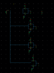
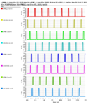
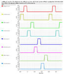
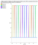
Simply I modified your netlist.
Then I ran modified netlist by Cadence Spectre.
See my netlist.
All informations are there.
Last edited:
 ) = -45.036 MA, took 70 ms.