Continue to Site
Follow along with the video below to see how to install our site as a web app on your home screen.
Note: This feature may not be available in some browsers.
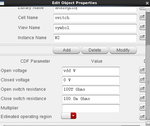
You will need to run a PAC analysis, I have read that sps may work as well
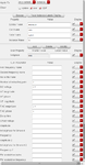
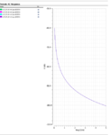
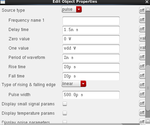
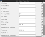
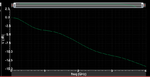
I did PSS+PAC however the response does not make sense to me ,I attach schematic and my simulation setup
do you have any idea that what is wrong with circuit?
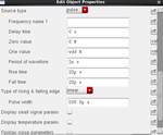
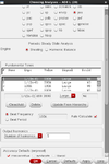
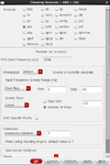
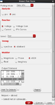
Pictures of GUI are very difficult to see for capturing your circumstances.I attach schematic and my simulation setup
do you have any idea that what is wrong with circuit?
Show me "input.scs".I do not know how can I get netlist?
Show me "input.scs".
No.this is my input
He doesn't have any pins in his schematic, so I don't think he has any inputs.No.
Show "input.scs".
Cadence ADE>Simulation>Netist>Recreate
Following is a example of "input.scs".
https://www.edaboard.com/threads/346180/
No.
Show "input.scs".
Cadence ADE>Simulation>Netist>Recreate
Following is a example of "input.scs".
https://www.edaboard.com/threads/346180/
// Generated for: spectre
// Generated on: Nov 11 22:09:39 2015
// Design library name: Assignment1_signalelectronic
// Design cell name: test_nasser4
// Design view name: schematic
simulator lang=spectre
global 0
parameters vdd=3.3
include "/CMC/kits/AMSKIT616_GPDK/tech/gpdk045_v_4_0/gpdk045/../models/spectre/gpdk045.scs" section=tt

// Library name: Assignment1_signalelectronic
// Cell name: test_nasser4
// View name: schematic
W3 (R0_MINUS C3_PLUS V4_PLUS 0) relay vt1=vdd vt2=0 ropen=100T \
        rclosed=100.0m
W1 (R0_MINUS C2_PLUS V2_PLUS 0) relay vt1=vdd vt2=0 ropen=100T \
        rclosed=100.0m
W0 (R0_MINUS C0_PLUS V1_PLUS 0) relay vt1=vdd vt2=0 ropen=100T \
        rclosed=100.0m
W2 (R0_MINUS C1_PLUS V3_PLUS 0) relay vt1=vdd vt2=0 ropen=100T \
        rclosed=100.0m
C3 (C3_PLUS 0) capacitor c=16p
C2 (C2_PLUS 0) capacitor c=16p
C0 (C0_PLUS 0) capacitor c=16p
C1 (C1_PLUS 0) capacitor c=16p
V4 (V4_PLUS 0) vsource type=pulse delay=1.5n edgetype=linear val0=0 \
        val1=vdd period=2n rise=50p fall=50p width=450p
V2 (V2_PLUS 0) vsource type=pulse delay=1n edgetype=linear val0=0 val1=vdd \
        period=2n rise=50p fall=50p width=450p
V1 (V1_PLUS 0) vsource type=pulse delay=500p edgetype=linear val0=0 \
        val1=vdd period=2n rise=50p fall=50p width=450p
V3 (V3_PLUS 0) vsource type=pulse delay=0 edgetype=linear val0=0 val1=vdd \
        period=2n rise=50p fall=50p width=450.0p
V0 (V0_PLUS 0) vsource dc=0 type=sine pacmag=1 pacphase=0
R0 (V0_PLUS R0_MINUS) resistor r=50K
simulatorOptions options reltol=1e-3 vabstol=1e-6 iabstol=1e-12 temp=27 \
    tnom=27 scalem=1.0 scale=1.0 gmin=1e-12 rforce=1 maxnotes=5 maxwarns=5 \
    digits=5 cols=80 pivrel=1e-3 sensfile="../psf/sens.output" \
    checklimitdest=psf
pss  pss  fund=500M  harms=5  errpreset=conservative  tstab=200u
+    maxacfreq=4G  annotate=status
pac  pac  start=50M  stop=5G  lin=1000  maxsideband=7
+    annotate=status
modelParameter info what=models where=rawfile
element info what=inst where=rawfile
outputParameter info what=output where=rawfile
designParamVals info what=parameters where=rawfile
primitives info what=primitives where=rawfile
subckts info what=subckts  where=rawfile
saveOptions options save=allpub// Generated for: spectre
// Generated on: Nov 11 22:58:23 2015
// Design library name: Assignment1_signalelectronic
// Design cell name: test_nasser4
// Design view name: schematic
simulator lang=spectre
global 0
parameters vdd=3.3
include "/CMC/kits/AMSKIT616_GPDK/tech/gpdk045_v_4_0/gpdk045/../models/spectre/gpdk045.scs" section=tt
// Library name: Assignment1_signalelectronic
// Cell name: test_nasser4
// View name: schematic
W3 (R0_MINUS C3_PLUS V4_PLUS 0) relay vt1=vdd vt2=0 ropen=100T \
rclosed=100.0m
W1 (R0_MINUS C2_PLUS V2_PLUS 0) relay vt1=vdd vt2=0 ropen=100T \
rclosed=100.0m
W0 (R0_MINUS C0_PLUS V1_PLUS 0) relay vt1=vdd vt2=0 ropen=100T \
rclosed=100.0m
W2 (R0_MINUS C1_PLUS V3_PLUS 0) relay vt1=vdd vt2=0 ropen=100T \
rclosed=100.0m
C3 (C3_PLUS 0) capacitor c=16p
C2 (C2_PLUS 0) capacitor c=16p
C0 (C0_PLUS 0) capacitor c=16p
C1 (C1_PLUS 0) capacitor c=16p
V4 (V4_PLUS 0) vsource type=pulse delay=1.5n edgetype=linear val0=0 \
val1=vdd period=2n rise=50p fall=50p width=450p
V2 (V2_PLUS 0) vsource type=pulse delay=1n edgetype=linear val0=0 val1=vdd \
period=2n rise=50p fall=50p width=450p
V1 (V1_PLUS 0) vsource type=pulse delay=500p edgetype=linear val0=0 \
val1=vdd period=2n rise=50p fall=50p width=450p
V3 (V3_PLUS 0) vsource type=pulse delay=0 edgetype=linear val0=0 val1=vdd \
period=2n rise=50p fall=50p width=450.0p
V0 (V0_PLUS 0) vsource dc=0 type=sine pacmag=1 pacphase=0
R0 (V0_PLUS R0_MINUS) resistor r=50K
simulatorOptions options reltol=1e-3 vabstol=1e-6 iabstol=1e-12 temp=27 \
tnom=27 scalem=1.0 scale=1.0 gmin=1e-12 rforce=1 maxnotes=5 maxwarns=5 \
digits=5 cols=80 pivrel=1e-3 sensfile="../psf/sens.output" \
checklimitdest=psf
pss pss fund=500M harms=0 errpreset=conservative tstab=200u
+ maxacfreq=4G annotate=status
pac pac start=50M stop=5G lin=1000 maxsideband=0
+ annotate=status
modelParameter info what=models where=rawfile
element info what=inst where=rawfile
outputParameter info what=output where=rawfile
designParamVals info what=parameters where=rawfile
primitives info what=primitives where=rawfile
subckts info what=subckts where=rawfile
saveOptions options save=allpub
You also can not understand Cadence Spectre Netlisting from Cadence ADE.He doesn't have any pins in his schematic, so I don't think he has any inputs.
Change these like following.V0 (V0_PLUS 0) vsource dc=0 type=sine pacmag=1 pacphase=0
pss pss fund=500M harms=5 errpreset=conservative tstab=200u
+ maxacfreq=4G annotate=status
pac pac start=50M stop=5G lin=1000 maxsideband=7
+ annotate=status
V0 (V0_PLUS 0) vsource dc=0 type=dc pacmag=1 pacphase=0
pss pss fund=500M harms=1 errpreset=conservative tstab=200u
+ maxacfreq=5G annotate=status
pac pac start=50M stop=5G lin=1000 maxsideband=0
+ annotate=status
db20( harmonic(v("/C0_PLUS", ?result "pac"), 0) )
db20( harmonic(v("/C1_PLUS", ?result "pac"), 0) )
db20( harmonic(v("/C2_PLUS", ?result "pac"), 0) )
db20( harmonic(v("/C3_PLUS", ?result "pac"), 0) )Plot followings.however result does not make sense to me again
[COLOR="#FF0000"]
db20(
   harmonic(v("/C0_PLUS", ?result "pac"), 0)
 +harmonic(v("/C1_PLUS", ?result "pac"), 0)
 +harmonic(v("/C2_PLUS", ?result "pac"), 0)
 +harmonic(v("/C3_PLUS", ?result "pac"), 0)
)

db20( harmonic(v("/R0_MINUS", ?result "pac"), 0) )[/COLOR]You also can not understand Cadence Spectre Netlisting from Cadence ADE.
When you run Cadence Spectre from Cadence ADE, netlist is created as "input.scs" in "simulation/<circuit_name>/spectre/schematic/netlist".
Analysis statements, Option statement and Signal source definitions are all described in "input.scs".
Change these like following.
Then plot followings.
db20( harmonic(v("/C0_PLUS", ?result "pac"), 0) )
db20( harmonic(v("/C1_PLUS", ?result "pac"), 0) )
db20( harmonic(v("/C2_PLUS", ?result "pac"), 0) )
db20( harmonic(v("/C3_PLUS", ?result "pac"), 0) )
Also see https://www.designers-guide.org/Forum/YaBB.pl?num=1258339986
You have to combine four outputs in schematic or post processing.
db20(
harmonic(v("/C0_PLUS", ?result "pac"), 0)
+harmonic(v("/C1_PLUS", ?result "pac"), 0)
+harmonic(v("/C2_PLUS", ?result "pac"), 0)
+harmonic(v("/C3_PLUS", ?result "pac"), 0)
)
// Generated for: spectre
// Generated on: Nov 11 22:58:23 2015
// Design library name: Assignment1_signalelectronic
// Design cell name: test_nasser4
// Design view name: schematic
simulator lang=spectre
global 0
parameters vdd=3.3
include "/CMC/kits/AMSKIT616_GPDK/tech/gpdk045_v_4_0/gpdk045/../models/spectre/gpdk045.scs" section=tt
// Library name: Assignment1_signalelectronic
// Cell name: test_nasser4
// View name: schematic
W3 (R0_MINUS C3_PLUS V4_PLUS 0) relay vt1=vdd vt2=0 ropen=100T \
rclosed=100.0m
W1 (R0_MINUS C2_PLUS V2_PLUS 0) relay vt1=vdd vt2=0 ropen=100T \
rclosed=100.0m
W0 (R0_MINUS C0_PLUS V1_PLUS 0) relay vt1=vdd vt2=0 ropen=100T \
rclosed=100.0m
W2 (R0_MINUS C1_PLUS V3_PLUS 0) relay vt1=vdd vt2=0 ropen=100T \
rclosed=100.0m
C3 (C3_PLUS 0) capacitor c=16p
C2 (C2_PLUS 0) capacitor c=16p
C0 (C0_PLUS 0) capacitor c=16p
C1 (C1_PLUS 0) capacitor c=16p
V4 (V4_PLUS 0) vsource type=pulse delay=1.5n edgetype=linear val0=0 \
val1=vdd period=2n rise=50p fall=50p width=450p
V2 (V2_PLUS 0) vsource type=pulse delay=1n edgetype=linear val0=0 val1=vdd \
period=2n rise=50p fall=50p width=450p
V1 (V1_PLUS 0) vsource type=pulse delay=500p edgetype=linear val0=0 \
val1=vdd period=2n rise=50p fall=50p width=450p
V3 (V3_PLUS 0) vsource type=pulse delay=0 edgetype=linear val0=0 val1=vdd \
period=2n rise=50p fall=50p width=450.0p
V0 (V0_PLUS 0) vsource dc=0 type=sine pacmag=1 pacphase=0
R0 (V0_PLUS R0_MINUS) resistor r=50K
simulatorOptions options reltol=1e-3 vabstol=1e-6 iabstol=1e-12 temp=27 \
tnom=27 scalem=1.0 scale=1.0 gmin=1e-12 rforce=1 maxnotes=5 maxwarns=5 \
digits=5 cols=80 pivrel=1e-3 sensfile="../psf/sens.output" \
checklimitdest=psf
pss pss fund=500M harms=0 errpreset=conservative tstab=200u
+ maxacfreq=4G annotate=status
pac pac start=50M stop=5G lin=1000 maxsideband=0
+ annotate=status
modelParameter info what=models where=rawfile
element info what=inst where=rawfile
outputParameter info what=output where=rawfile
designParamVals info what=parameters where=rawfile
primitives info what=primitives where=rawfile
subckts info what=subckts where=rawfile
saveOptions options save=allpub
You also can not understand Cadence Spectre Netlisting from Cadence ADE.
When you run Cadence Spectre from Cadence ADE, netlist is created as "input.scs" in "simulation/<circuit_name>/spectre/schematic/netlist".
Analysis statements, Option statement and Signal source definitions are all described in "input.scs".
Change these like following.
Then plot followings.
db20( harmonic(v("/C0_PLUS", ?result "pac"), 0) )
db20( harmonic(v("/C1_PLUS", ?result "pac"), 0) )
db20( harmonic(v("/C2_PLUS", ?result "pac"), 0) )
db20( harmonic(v("/C3_PLUS", ?result "pac"), 0) )
Also see https://www.designers-guide.org/Forum/YaBB.pl?num=1258339986
Plot followings.
db20(
harmonic(v("/C0_PLUS", ?result "pac"), 0)
+harmonic(v("/C1_PLUS", ?result "pac"), 0)
+harmonic(v("/C2_PLUS", ?result "pac"), 0)
+harmonic(v("/C3_PLUS", ?result "pac"), 0)
)
db20( harmonic(v("/R0_MINUS", ?result "pac"), 0) )
db(vh('pac "/C3_PLUS" '(0)))+(db(vh('pac "/C2_PLUS" '(0)))+(db(vh('pac "/C0_PLUS" '(0)))+db(vh('pac "/C1_PLUS" '(0)))))No.you mean this:
db(vh('pac "/C3_PLUS" '(0)))+(db(vh('pac "/C2_PLUS" '(0)))+(db(vh('pac "/C0_PLUS" '(0)))+db(vh('pac "/C1_PLUS" '(0)))))
db(
vh('pac "/C3_PLUS" '(0))
+vh('pac "/C2_PLUS" '(0))
+vh('pac "/C0_PLUS" '(0))
+vh('pac "/C1_PLUS" '(0))
)you mean this:No.
See surely equation I appended.
Add as complex number and apply db20() for results.
Code:db( vh('pac "/C3_PLUS" '(0)) +vh('pac "/C2_PLUS" '(0)) +vh('pac "/C0_PLUS" '(0)) +vh('pac "/C1_PLUS" '(0)) )
No.you mean this:
db20(harmonic(v("/C0_PLUS" ?result "pac") 0))+db20( harmonic(v("/C2_PLUS", ?result "pac"), 0) )+db20( harmonic(v("/C3_PLUS", ?result "pac"), 0) )+db20( harmonic(v("/C1_PLUS", ?result "pac"), 0) )Code:
simulator lang=spectre
global 0
parameters vdd=3.3
parameters vt1=vdd/2*(1-1e-3)
parameters vt2=vdd/2*(1+1e-3)

V0 (V0_PLUS 0) vsource dc=0 type=dc pacmag=1 pacphase=0
R0 (V0_PLUS R0_MINUS) resistor r=50K

V1 (V1_PLUS 0) vsource type=pulse delay=500p edgetype=linear \
val0=0 val1=vdd period=2n rise=50p fall=50p width=450p
V2 (V2_PLUS 0) vsource type=pulse delay=1n edgetype=linear \
val0=0 val1=vdd period=2n rise=50p fall=50p width=450p
V3 (V3_PLUS 0) vsource type=pulse delay=0 edgetype=linear \
val0=0 val1=vdd period=2n rise=50p fall=50p width=450p
V4 (V4_PLUS 0) vsource type=pulse delay=1.5n edgetype=linear \
val0=0 val1=vdd period=2n rise=50p fall=50p width=450p

W0 (R0_MINUS C0_PLUS V1_PLUS 0) relay vt1=vt1 vt2=vt2 \
ropen=100T rclosed=100.0m
W1 (R0_MINUS C2_PLUS V2_PLUS 0) relay vt1=vt1 vt2=vt2 \
ropen=100T rclosed=100.0m
W2 (R0_MINUS C1_PLUS V3_PLUS 0) relay vt1=vt1 vt2=vt2 \
ropen=100T rclosed=100.0m
W3 (R0_MINUS C3_PLUS V4_PLUS 0) relay vt1=vt1 vt2=vt2 \
ropen=100T rclosed=100.0m

C0 (C0_PLUS 0) capacitor c=16p
C1 (C1_PLUS 0) capacitor c=16p
C2 (C2_PLUS 0) capacitor c=16p
C3 (C3_PLUS 0) capacitor c=16p

simulatorOptions options reltol=1e-3 vabstol=1e-6 iabstol=1e-12 temp=27 \
tnom=27 scalem=1.0 scale=1.0 gmin=1e-12 rforce=1 maxnotes=5 maxwarns=5 \
digits=5 cols=80 pivrel=1e-3 sensfile="../psf/sens.output" \
checklimitdest=psf

pss pss fund=500M harms=0 errpreset=conservative
+ tstab=200u maxacfreq=5G
+ annotate=status

pac pac start=50M stop=5G lin=1000 maxsideband=0
+ annotate=status

saveOptions options save=allpubpsf_dir = strcat("/tmp/", "/hoge.raw")
openResults(psf_dir)
selectResult("pac")
R0_MINUS = harmonic( v("R0_MINUS"), 0 )
plot( db20(R0_MINUS) )
C0_PLUS = harmonic( v("C0_PLUS"), 0 )
C1_PLUS = harmonic( v("C1_PLUS"), 0 )
C2_PLUS = harmonic( v("C2_PLUS"), 0 )
C3_PLUS = harmonic( v("C3_PLUS"), 0 )
Csum_PLUS = C0_PLUS + C1_PLUS + C2_PLUS + C3_PLUS
plot( db20(Csum_PLUS) )This is a netlist I used.The following is a OCEAN script for plotting.Code:simulator lang=spectre global 0 parameters vdd=3.3 parameters vt1=vdd/2*(1-1e-3) parameters vt2=vdd/2*(1+1e-3) V0 (V0_PLUS 0) vsource dc=0 type=dc pacmag=1 pacphase=0 R0 (V0_PLUS R0_MINUS) resistor r=50K V1 (V1_PLUS 0) vsource type=pulse delay=500p edgetype=linear \ val0=0 val1=vdd period=2n rise=50p fall=50p width=450p V2 (V2_PLUS 0) vsource type=pulse delay=1n edgetype=linear \ val0=0 val1=vdd period=2n rise=50p fall=50p width=450p V3 (V3_PLUS 0) vsource type=pulse delay=0 edgetype=linear \ val0=0 val1=vdd period=2n rise=50p fall=50p width=450p V4 (V4_PLUS 0) vsource type=pulse delay=1.5n edgetype=linear \ val0=0 val1=vdd period=2n rise=50p fall=50p width=450p W0 (R0_MINUS C0_PLUS V1_PLUS 0) relay vt1=vt1 vt2=vt2 \ ropen=100T rclosed=100.0m W1 (R0_MINUS C2_PLUS V2_PLUS 0) relay vt1=vt1 vt2=vt2 \ ropen=100T rclosed=100.0m W2 (R0_MINUS C1_PLUS V3_PLUS 0) relay vt1=vt1 vt2=vt2 \ ropen=100T rclosed=100.0m W3 (R0_MINUS C3_PLUS V4_PLUS 0) relay vt1=vt1 vt2=vt2 \ ropen=100T rclosed=100.0m C0 (C0_PLUS 0) capacitor c=16p C1 (C1_PLUS 0) capacitor c=16p C2 (C2_PLUS 0) capacitor c=16p C3 (C3_PLUS 0) capacitor c=16p simulatorOptions options reltol=1e-3 vabstol=1e-6 iabstol=1e-12 temp=27 \ tnom=27 scalem=1.0 scale=1.0 gmin=1e-12 rforce=1 maxnotes=5 maxwarns=5 \ digits=5 cols=80 pivrel=1e-3 sensfile="../psf/sens.output" \ checklimitdest=psf pss pss fund=500M harms=0 errpreset=conservative + tstab=200u maxacfreq=5G + annotate=status pac pac start=50M stop=5G lin=1000 maxsideband=0 + annotate=status saveOptions options save=allpubThere is no output sampler in your circuit.Code:psf_dir = strcat("/tmp/", "/hoge.raw") openResults(psf_dir) selectResult("pac") R0_MINUS = harmonic( v("R0_MINUS"), 0 ) plot( db20(R0_MINUS) ) C0_PLUS = harmonic( v("C0_PLUS"), 0 ) C1_PLUS = harmonic( v("C1_PLUS"), 0 ) C2_PLUS = harmonic( v("C2_PLUS"), 0 ) C3_PLUS = harmonic( v("C3_PLUS"), 0 ) Csum_PLUS = C0_PLUS + C1_PLUS + C2_PLUS + C3_PLUS plot( db20(Csum_PLUS) )
So C0_PLUS, C1_PLUS, C2_PLUS and C3_PLUS are all in-phase.
can you please send me your schematic and you pss+pac setup ?This is a netlist I used.The following is a OCEAN script for plotting.Code:simulator lang=spectre global 0 parameters vdd=3.3 parameters vt1=vdd/2*(1-1e-3) parameters vt2=vdd/2*(1+1e-3) V0 (V0_PLUS 0) vsource dc=0 type=dc pacmag=1 pacphase=0 R0 (V0_PLUS R0_MINUS) resistor r=50K V1 (V1_PLUS 0) vsource type=pulse delay=500p edgetype=linear \ val0=0 val1=vdd period=2n rise=50p fall=50p width=450p V2 (V2_PLUS 0) vsource type=pulse delay=1n edgetype=linear \ val0=0 val1=vdd period=2n rise=50p fall=50p width=450p V3 (V3_PLUS 0) vsource type=pulse delay=0 edgetype=linear \ val0=0 val1=vdd period=2n rise=50p fall=50p width=450p V4 (V4_PLUS 0) vsource type=pulse delay=1.5n edgetype=linear \ val0=0 val1=vdd period=2n rise=50p fall=50p width=450p W0 (R0_MINUS C0_PLUS V1_PLUS 0) relay vt1=vt1 vt2=vt2 \ ropen=100T rclosed=100.0m W1 (R0_MINUS C2_PLUS V2_PLUS 0) relay vt1=vt1 vt2=vt2 \ ropen=100T rclosed=100.0m W2 (R0_MINUS C1_PLUS V3_PLUS 0) relay vt1=vt1 vt2=vt2 \ ropen=100T rclosed=100.0m W3 (R0_MINUS C3_PLUS V4_PLUS 0) relay vt1=vt1 vt2=vt2 \ ropen=100T rclosed=100.0m C0 (C0_PLUS 0) capacitor c=16p C1 (C1_PLUS 0) capacitor c=16p C2 (C2_PLUS 0) capacitor c=16p C3 (C3_PLUS 0) capacitor c=16p simulatorOptions options reltol=1e-3 vabstol=1e-6 iabstol=1e-12 temp=27 \ tnom=27 scalem=1.0 scale=1.0 gmin=1e-12 rforce=1 maxnotes=5 maxwarns=5 \ digits=5 cols=80 pivrel=1e-3 sensfile="../psf/sens.output" \ checklimitdest=psf pss pss fund=500M harms=0 errpreset=conservative + tstab=200u maxacfreq=5G + annotate=status pac pac start=50M stop=5G lin=1000 maxsideband=0 + annotate=status saveOptions options save=allpubThere is no output sampler in your circuit.Code:psf_dir = strcat("/tmp/", "/hoge.raw") openResults(psf_dir) selectResult("pac") R0_MINUS = harmonic( v("R0_MINUS"), 0 ) plot( db20(R0_MINUS) ) C0_PLUS = harmonic( v("C0_PLUS"), 0 ) C1_PLUS = harmonic( v("C1_PLUS"), 0 ) C2_PLUS = harmonic( v("C2_PLUS"), 0 ) C3_PLUS = harmonic( v("C3_PLUS"), 0 ) Csum_PLUS = C0_PLUS + C1_PLUS + C2_PLUS + C3_PLUS plot( db20(Csum_PLUS) )
So C0_PLUS, C1_PLUS, C2_PLUS and C3_PLUS are all in-phase.