Continue to Site

Welcome to EDAboard.com

Welcome to our site! EDAboard.com is an international Electronics Discussion Forum focused on EDA software, circuits, schematics, books, theory, papers, asic, pld, 8051, DSP, Network, RF, Analog Design, PCB, Service Manuals... and a whole lot more! To participate you need to register. Registration is free. Click here to register now.

[moved] 2 stage CMOS OP-AMP design in Cadence

Status
Not open for further replies.

sumovow

Newbie level 1
Joined
Feb 5, 2016
Messages
1
Helped
0
Reputation
0
Reaction score
0
Trophy points
1
Activity points
12
op-amp.png

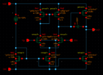
I have designed an op-amp in Cadence with 45nm technology process file(gpdk045) as shown in the picture. VDD is provided 1V. But I am not getting desired output while transient analysis (both inverting and non-inverting mode). Can anyone please help me on this. Should I change any parameter or anything. It will be also helpful if anyone can suggest different type of Op-amp design. (in Cadence). Thank You
 

Did you adjust current less/more through NM0, until you obtain voltage changes at the node between PM0 & NM4 (the output of your differential amplifier)?
 

Show your test circuit incl. Vp, Vm connections and node voltages! What's your desired output?
 

Status
Not open for further replies.

Part and Inventory Search

Welcome to EDABoard.com

Sponsor

Back
Top