mirror_pole
Member level 3
Hello guys,
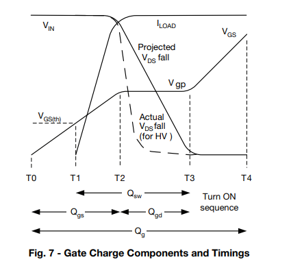
I have some questions related to the attached diagramm. The diagramm represents the turn on process of a MOSFET with an inductive load.
1) T1-T2: After UGS reaches Vth, MOSFET starts to conduct. Why does VDS stay constant until T2? I assumed that as soon as the MOSFET starts to conduct, the VDS voltage starts to decrease. My only guess would be that since i have an inductive load, the change in Drain current induces a voltage of opposite direction. This effect keeps the drain voltage at the initial level, as long as the current is varrying with time. After T2 the current is constant, so the inductor is acting as a short and the drain voltage begins to decrease. Im not sure if my assumption is correct.
2) T2-T3: I understood that because of the miller effect, and therefore the big Cgd seeing from the input, the whole current provided to the Gate charges Cgd => VGS stays constant for that time. At the same time VDS is going down. Why does the current stay constant here? I thought that the current is dependent on VGS and VDS. Im assuming that i can refere to the standard equations for the drain current from the MOS Level 1 model. But im not sure if i can use this equations here.
3) I also dont quit understand the loading of the Cgd. In the initial state, when the MOSFET is off and there is no current, Cgd should be loaded to Vin right? Does the charging of Cgd already start from the begining? And why do i even have a plateau for VGS? Why does the whole current charges up Cgd and no charge to Cgs at some point?
4) What are the operating regions for the different time frames? I assumed that during T2-T3 im operating in the linear region, since VDS is decreasing and therefore rd (channel res) is decreasing. Do i operate in saturation region from T3 on?