Continue to Site

Welcome to EDAboard.com

Welcome to our site! EDAboard.com is an international Electronics Discussion Forum focused on EDA software, circuits, schematics, books, theory, papers, asic, pld, 8051, DSP, Network, RF, Analog Design, PCB, Service Manuals... and a whole lot more! To participate you need to register. Registration is free. Click here to register now.

[SOLVED] Full-Bridge CLLC, high-side Mosfet Vgs self-turn-on

Status
Not open for further replies.

kinghero89

Junior Member level 2
Joined
Aug 8, 2023
Messages
23
Helped
0
Reputation
0
Reaction score
0
Trophy points
1
Activity points
130
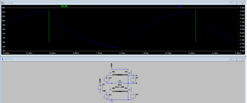
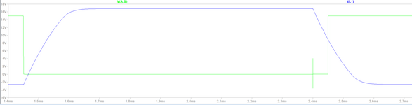
I am working on full-bridge CLLC, and the waveform I got is quite weird.
Is there anyone who has such kind of experience?

Screenshot 2023-08-08 230207.png
 

Solution
Cảm ơn mọi người đã hỗ trợ, tôi bố trí lại PCB và sử dụng gói Mosfet 4 chân và nhận được kết quả tốt hơn.

Thanks everyone for the support, I rearranged the PCB and used a 4-pin Mosfet package and got better results.
Lack of information
circuit topology? secondary rectifier or active bridge?
timing of low side gate signal?
gate driver strength?
do we see self commutation after low-side switch-off?
 

Lack of information
circuit topology? secondary rectifier or active bridge?
timing of low side gate signal?
gate driver strength?
do we see self commutation after low-side switch-off?
This is the schematic and gate driver I am using

driver.png

circuit1.png
 

Lack of information
circuit topology? secondary rectifier or active bridge?
timing of low side gate signal?
gate driver strength?
do we see self commutation after low-side switch-off?
This happens at the active bridge, Thank you for your answer
 

You need Ciss >> Cgd. But also a powerful enough gate drive to hard short the gate to ground when the fet should be off.
But also, probe it with a homebrew coaxial probe because it could just be a common mode spike.
Beware isolation with a coaxial probe and your scope.
The standard scope "dangly ground" probe thing is good at producing fake artifacts that are really just common mode illusions.
 

This is a common experience for power electronics newbies, when the high side turns on the drain of the lower is pulled up rapidly, injecting current into the lower gate via Cgd

If the gate drive does not have a low Z to these high freq edges it cannot keep the Vgs down.

[ vice versa is true for high side GD when lower device turns on fast ]
thanks for your answer, the gate drive i am using has the maximum current up to 3A
You need Ciss >> Cgd. But also a powerful enough gate drive to hard short the gate to ground when the fet should be off.
But also, probe it with a homebrew coaxial probe because it could just be a common mode spike.
Beware isolation with a coaxial probe and your scope.
The standard scope "dangly ground" probe thing is good at producing fake artifacts that are really just common mode illusions.
I use MOSFET with Ciss = 1500pF and Cgd = 2.6pF, the maximum current of gate driver can be up to 3A as I posted earlier
 

short the probe together, and connect that to the gate...do you still see the spike?..if so, then its common mode noise.
Also, how is your layout...i hope gate drive loop is not big in area?
Sometimes people slow the top gate drive, say, to stop the bottom gate drive turning on spuriously, and vice versa.
 

Several questions are still open. Low side gate timing? Gate series resistors? Is it right that we see passive commutation after low side switch-off?
 

Several questions are still open. Low side gate timing? Gate series resistors? Is it right that we see passive commutation after low side switch-off?
The turn-on resistor is 12 Ohm, the turn-off resistor is 22 Ohm.
The attached picture is the waveform of the low-side switch

aaa.png
 

" thanks for your answer, the gate drive i am using has the maximum current up to 3A "

It is not so much the claimed current capability - but rather the speed of the circuit in being able to handle very fast edges on the gate - in this case clamping gate rise - very few IC designers have a good handle on this.
--- Updated ---

22 ohms is a little high for turn off unless your gate driver has an extra pin to clamp the gate to source just following the soft turn off provided by the 22 ohms,

if the spike current in the 22 ohm resistor is say 200mA when the upper device turns on ( say) then the gate rise will be 4.4 volts.

If no special clamp, then it is usual to use a reverse schottky to allow the gate drive to pull the gate to source without an intervening resistor to mess things up.

p.s. Cgd is not a static figure.
 
Last edited:

I agree with Easy peasy. Problem is the inappropriately high Roff gate resistor. You really need strong gate clamping without negative gate voltage.
 

I agree with Easy peasy. Problem is the inappropriately high Roff gate resistor. You really need strong gate clamping without negative gate voltage.
because i want to reduce the high dv/dt of Vds so i increase the Roff gate resistor. The phenomenon I mentioned occurs at the start of deadtime interval, when the primary current discharges the Vds voltage of the lower Mosfet rapidly may interfere the Vgs voltage of the upper Mosfet. Do you have any idea about it?
 

According to the simulation, the Vgs voltage spikes are negative. Do u guys have any idea?
 

Attachments

  • simulaion.png
    simulaion.png
    47.1 KB · Views: 67

you appear to be missing the point, a simple diode S -> G would stop any neg spikes on the gate

it is the gate rise when the other device turns on that you should be concerned with
--- Updated ---

it is hard to see as you have not zoomed in - but the gate spike ( rise ) might be largely artifact too - due to probing. ( on your low side pictures )
I am thinking of the parasitic inductance
 

Attachments

  • Simulation2.png
    Simulation2.png
    30.1 KB · Views: 63

Also agree that the high turn-off resistor is likely the culprit. In most cases, for a unipolar gate driver, the Roff is lower than Ron.

In your example, your gate driver outputs 0-15V, and the FET switches with Vgs around 6V. So during turn-on the voltage across the gate resistance will be 9V, whereas during turn-off it will be 6V. So to get equal gate current during both edges you would Ron = 1.5*Roff.

This isn't necessarily an optimal method of choosing values, but if you're going in the opposite direction you should probably have a good reason for it...
--- Updated ---

According to the simulation, the Vgs voltage spikes are negative. Do u guys have any idea?
Be careful about looking to simulations to investigate this sort of issue. There are many possible mechanisms for spikes (positive or negative) to appear where you're observing them. And in practice what we actually observe in real life is a combination of several mechanisms, not just one. So don't jump to conclusions just because LTspice showed something interesting.

The LTspice schematic you showed isn't a good representation of your actual circuit. Try using the correct device model, and putting the Ron/Roff resistances in.
 
Last edited:
According to the simulation, the Vgs voltage spikes are negative. Do u guys have any idea?
You are right, you don't expect positive miller effect induced gate pulse when Vds is falling. It's more likely a measurement artifact, e.g. common mode error of the differential voltage probe. How do you exactly probe high side Vgs?
 
You are right, you don't expect positive miller effect induced gate pulse when Vds is falling. It's more likely a measurement artifact, e.g. common mode error of the differential voltage probe. How do you exactly probe high side Vgs?
I am pretty sure there’s spikes. At the beginning, i thought it was the differential voltage probe error. I increased the load current to 4.5 A, the spike might be higher leading to self turn-on of Vgs and the Mosfet was broken.
 

Status
Not open for further replies.

Part and Inventory Search

Welcome to EDABoard.com

Sponsor

Back
Top