kinghero89
Junior Member level 2
I am working on full-bridge CLLC, and the waveform I got is quite weird.
Is there anyone who has such kind of experience?

Is there anyone who has such kind of experience?
Follow along with the video below to see how to install our site as a web app on your home screen.
Note: This feature may not be available in some browsers.
I suspect the parasitic inductance of gs may cause the problem. The gate driver I used has max. current up to 3A, and i even didn’t use turn off resistor, just used an bypass diode, and the spike is still there.Sounds like you need a decent gate drive with low ohms ( turn off ) to ensure the device stays OFF.
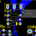
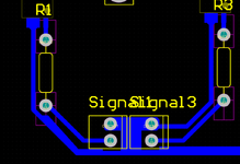
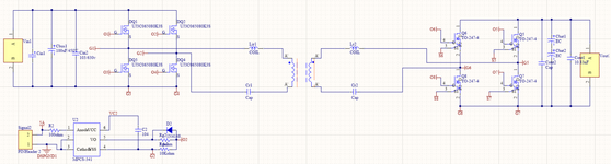
My PCB layout might not be good enough. Please have a look at it and give me some comments. Thank you.There are many things that can be done to narrow down the cause of observed spikes. The parasitic inductance explanation sounds implausible to me, unless it's a weird circuit layout. But we need to see the layout details to check.
Another possible reason that should be considered is switching noise affecting the gate driver input side.
To check if the transistor is actually turning on, I would observe drain current with a suitable probe, e.g. small Rogowski coil.
in the beginning, I used 5.1 Ohm resistor to turn on MOSFET, the waveform you see earlier I used 11 Ohm to turn on MOSFET.it's no surprise if the gate driver impedance cannot hack the high frequencies involved in the gate rise scenario - relatively few are good here - have you tried a slower turn on in the fets . . . ?
I used a separate controller board and connect to gate driver by twisting signal wire and header. The switching frequency is up to 160kHz. Is there anyway to reduce the spike?Good that you identified gate driver input signal as primary issue. According to post #3 schematic the single ended signal is connected through a pin header and possibly a cable, this will not necessarily work in a fast switching power stage.
There is only an 100 ohm resistor connected to 5A to reduce the current goes through the input of the gate driver.Torroid core as common mode choke might help. Anything connected to DSPGND1 and 5A on the power board?
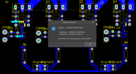
Yes, it looks like thisMeans each gate driver has it's own ground connected through header?
No, grounds are tied together. Might introduce additional common noise and is definitely a problem when you try to add common mode chokes.Yes, it looks like this
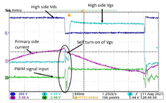
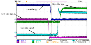
No, Vds,hs and Vds,ls are expected to transit simultaneously. As usual for a soft switching inverter, Vds commutation occurs after low-side switch off.Noted re dead time, but it appeared to be almost zero here:
It's quite fast for soft switching, but as far as I see determined by magnetizing current and Cds. It could be slowed down by switching FETs off extra-slow, unusual for soft-switching converter and mainly causing unwanted losses.Do you guys think MOSFETs' rise and fall time is too fast? Should I reduce it to reduce the spike?
I understand. This is my schematic and gate driver layout PCB. The GND should be seperated. I will modify it and test it again. Thank you for your information.my assumption here is that the gate drive IC is very far away from the devices - without seeing the whole it is very difficult to offer cogent advice.
The poster should not drip feed information - but rather make a clean breast of the schematic and photo's to clarify.
This would stop a lot of wasted time with back & forth ....
Yes, you are right. Because I want the soft-switching waveform more clearly so I increased the magnetizing current. Do you think it is too high (about 12A max) for a full load of 2kW? By the way, the resonant inductor of the active bridge gets hot (up to 100 C degree ) when the converter runs for about 2 mins. Is it due to the high resonant current?No, grounds are tied together. Might introduce additional common noise and is definitely a problem when you try to add common mode chokes.
No, Vds,hs and Vds,ls are expected to transit simultaneously. As usual for a soft switching inverter, Vds commutation occurs after low-side switch off.
It's quite fast for soft switching, but as far as I see determined by magnetizing current and Cds. It could be slowed down by switching FETs off extra-slow, unusual for soft-switching converter and mainly causing unwanted losses.