Continue to Site

Welcome to EDAboard.com

Welcome to our site! EDAboard.com is an international Electronics Discussion Forum focused on EDA software, circuits, schematics, books, theory, papers, asic, pld, 8051, DSP, Network, RF, Analog Design, PCB, Service Manuals... and a whole lot more! To participate you need to register. Registration is free. Click here to register now.

N Channel MOSFET Turn On Behaviour

Status
Not open for further replies.

vaibhavwaman

Newbie level 4
Joined
Dec 26, 2009
Messages
7
Helped
0
Reputation
0
Reaction score
0
Trophy points
1,281
Location
mumbai
Activity points
1,369
Hello,

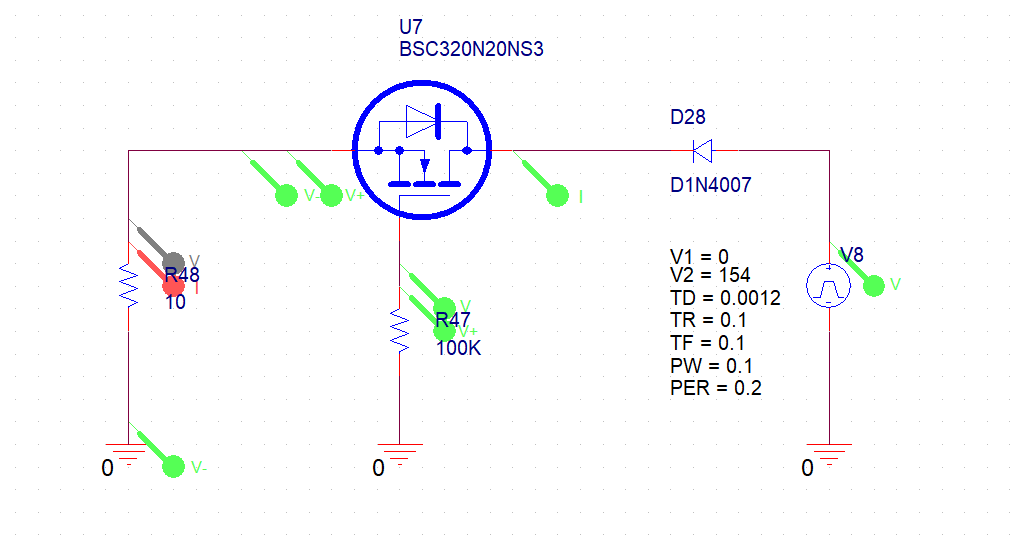
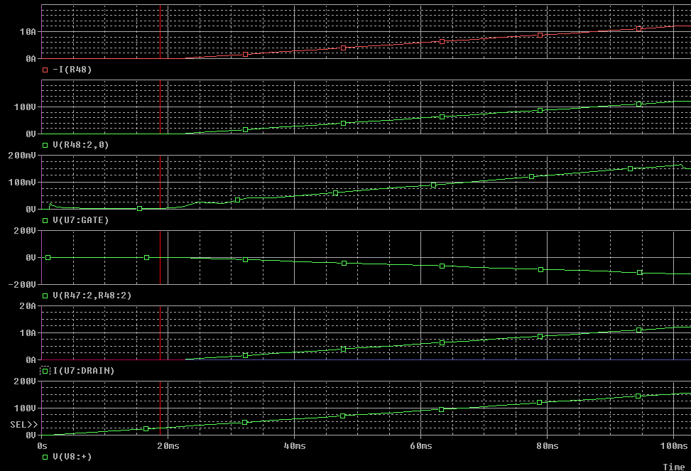
When I simulated below N channel MOSFET circuit, I observed though MOSFET is connect to ground it starts conducting from Drain to source after ~30V ? why this is happening ?

This MOSFET has 200V VDS breakdown voltage but still it conducts far earlier. Rise time of Drain voltage is also not much high to cause breakdown.
1665572775443.png


1665572919069.png
 

Since your x axis is time are you looking at the trasnsient response due to
MOSFET parasitic C ? Should you be looking at a DC sweep of V ?


Regards, Dana.
 

Yes, as the above noticed....change R47 to zero ohms and notice it doesnt happen so much....but also remember the drain-source capacitance. As the above members have already said.
Google "Spurious FET turn ON" for more info
 
Last edited:

None of the explanations makes sense. You don't turn the transistor on at 1.5 V/ms Vds slope. Cgd related turn on would show in V(U7:G), but there's no significant voltage rise. Initial 20 mV peak is realistic according to Vds slope. Drain current starting at about 30V Vds isn't gate triggered, apparently Vds breakdown.

My assumption: defective model. I don't have a recent PSPICE version with BSC320N20 model. Please post netlist (generated .cir file) and transistor model file.
 

Status
Not open for further replies.

Similar threads

Part and Inventory Search

Welcome to EDABoard.com

Sponsor

Back
Top