Continue to Site

Welcome to EDAboard.com

Welcome to our site! EDAboard.com is an international Electronics Discussion Forum focused on EDA software, circuits, schematics, books, theory, papers, asic, pld, 8051, DSP, Network, RF, Analog Design, PCB, Service Manuals... and a whole lot more! To participate you need to register. Registration is free. Click here to register now.

Misplacement of layers in Altium

Status
Not open for further replies.

vidivici.world

Junior Member level 3
Joined
Nov 10, 2009
Messages
31
Helped
0
Reputation
0
Reaction score
0
Trophy points
1,286
Activity points
1,490
Hi, I was drawing the PCB files in Altium and found something weird.
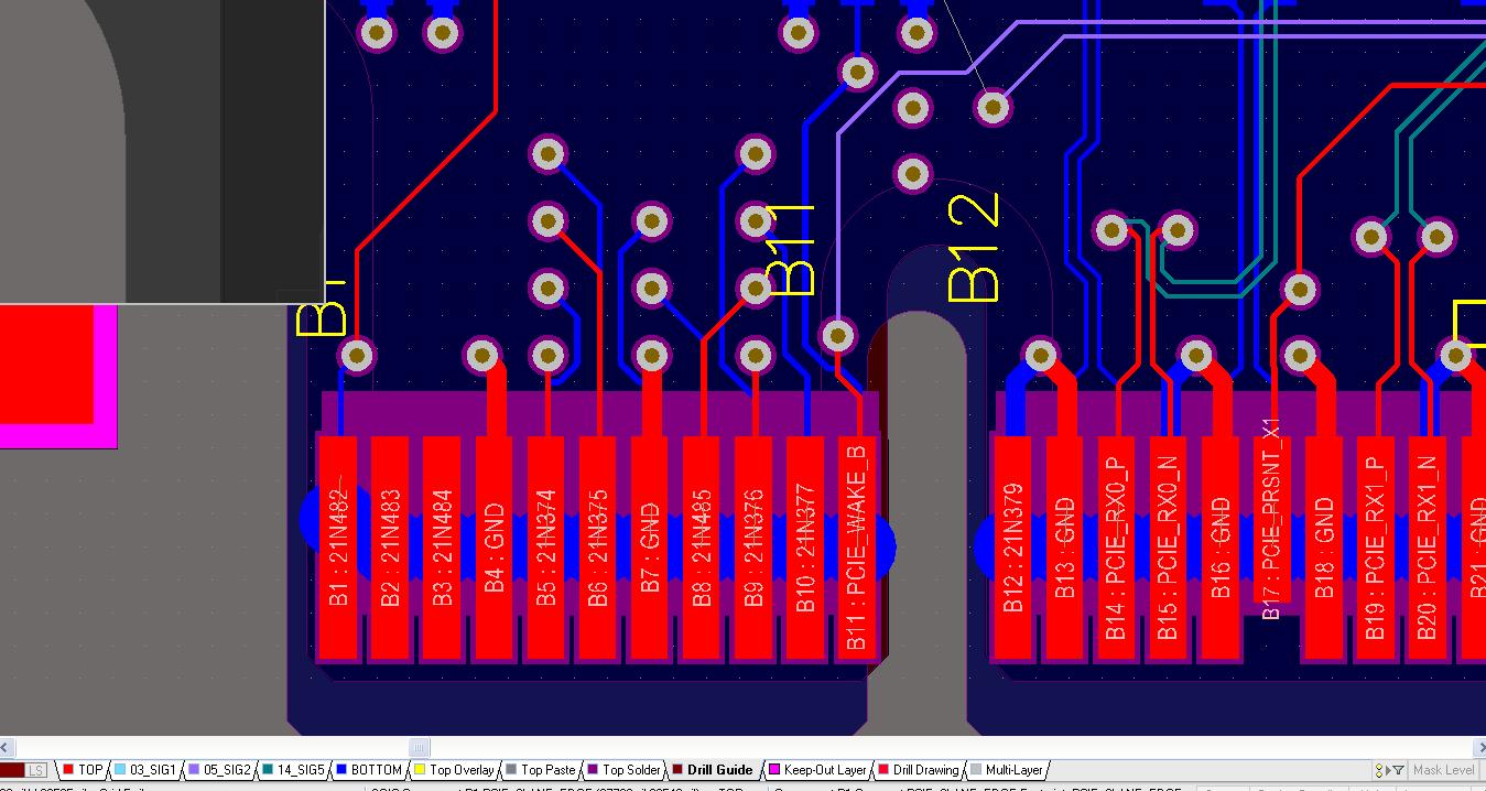
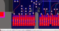
The coordinates of layers seem to be different, as show in the picture. The drill guide layer is not right below the other layer, but a little misplaced.
Is there some way to adjust this layer to the right position? thanks a lot!
 

it looks like your board shape is off. you will need to redefine the new board shape.
 

It is not very clear from the image what exactly is the problem, but if it is only one layer that is drill guide than it must be after you have generated the gerbers you have to check your fabrication settings for that.
You have to keep your drill and gerber fabrication settings same while generating gerber files.
Hope this helps you otherwise please elaborate your problem little more.
 

thanks for your reply! I have solved my problem, by moving the layer in my PCB file.
But you mentioned "keep your drill and gerber fabrication settings same" , will the position of drills in gerber files be different from these in PCB files, if some settings are not correct?
 

By "keep your drill and gerber fabrication settings same" I mean to say that NC Drill settings and arrtwork settings should be same otherwise in gerber it will be misaligned
 

Status
Not open for further replies.

Part and Inventory Search

Welcome to EDABoard.com

Sponsor

Back
Top