Continue to Site

Welcome to EDAboard.com

Welcome to our site! EDAboard.com is an international Electronics Discussion Forum focused on EDA software, circuits, schematics, books, theory, papers, asic, pld, 8051, DSP, Network, RF, Analog Design, PCB, Service Manuals... and a whole lot more! To participate you need to register. Registration is free. Click here to register now.

[SOLVED] MAX485. There is a small question of application.

Status
Not open for further replies.

gherkins

Newbie level 5
Joined
Aug 20, 2015
Messages
9
Helped
0
Reputation
0
Reaction score
0
Trophy points
1
Activity points
70
Hello everyone!

there is a small question of application MAX485.
Probably somebody knows or can explain the first variant of application: ic1.png

Probably somebody knows or can explain the second one: ic2.png
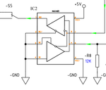
In the first application I am interesting in why they use shottky diode with pins 2,3 together. Is it application of constant transmission?

In the second application I am interesting in why the all the pins 2,3,4 sit on the ground there. Is it application of constant receiving?


thanks in advance!
 
Last edited:

Hi,

1) the schottky diodde pretects the input against negative voltage.

2) The circuit is only used as receiver. Never as transmitter.

Klaus
 

and first circuit is used as constant transmitter?
 

-RE is the receiver enable control. When low the receiver output is enabled and data appears on RO.
DE is the driver enable control, when high the DI signal is sent to the line, when low, the driver outputs are disabled.

The polarities are opposites simply to make it easier to use, they can be linked if necessary and then used as a single transmit/receive signal.

The first circuit uses switch S6 to pull the control line to +5V, which would make the transmitter active but the design is bad, when the switch is open there is nothing to pull the voltage low again. The diode should really be a pull-down resistor.

Brian.
 

no, regarding to IC1 the S6 is allways in the state as shown. The IC1 pins 2,3 an diode sit on the TTL signal line is coming from DB25 pin 22.
 

In that case, DB25 pin 22 conrtols whether it transmits or receives and the diode is (hopefully) going to clamp any negative voltage transitions. It would be prudent to add a small resistor in series with pin 22 or the diode could be asked to sink considerable current.

Brian.
 

Status
Not open for further replies.

Part and Inventory Search

Welcome to EDABoard.com

Sponsor

Back
Top