Continue to Site

Welcome to EDAboard.com

Welcome to our site! EDAboard.com is an international Electronics Discussion Forum focused on EDA software, circuits, schematics, books, theory, papers, asic, pld, 8051, DSP, Network, RF, Analog Design, PCB, Service Manuals... and a whole lot more! To participate you need to register. Registration is free. Click here to register now.

LTC3783 step-up LED driver

ArticCynda

Advanced Member level 1
Joined
May 8, 2013
Messages
439
Helped
82
Reputation
164
Reaction score
81
Trophy points
1,308
Activity points
4,238
Hi everyone,

I'd like some input and/or second opinion from those among you who are experienced with switched mode DC/DC converters, please!

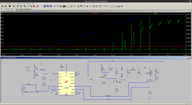
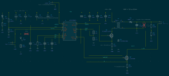
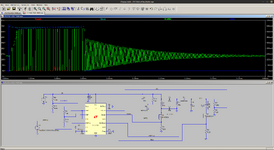
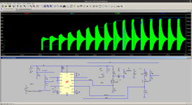
I'm working on a LED driver that runs strings of LEDs at 72 V with a forward current of 600 mA, designed to run from a 24 V DC supply. See circuit and sim results below. Blue curve shows output voltage (rectified secondary transformer winding) and green curve shows current through the LEDs. The circuit design follows datasheet guidelines, and works exactly as expected in LTSpice where it produces 72 V output at 600 mA forward current, and can be very nicely PWM'ed.

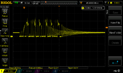
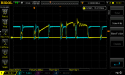
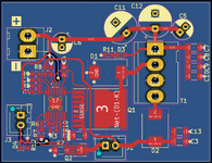
Unfortunately, the prototype doesn't work. When the RUN threshold voltage is applied to turn on the LTC3783 controller, oscilloscope on primary transformer winding shows there is no switching happening at all. Instead, the LTC3783 gets really hot in just a few seconds, and the circuit draws ca. 150 mA from the 24 V supply rail. The only difference between simulation and prototype is that I swapped the Si4470 Vishay MOSFET for Infineon IPT015N10NF2S MOSFET, due to unavailability of the Vishay ones.

Any suggestions on where to start debugging this? All ideas/tips are most appreciated.

Thanks,

AC

1706138388302.png
 
..so you are trying to do flyback?....what is the coupled inductor that you use?
What is LTC3783 gate drive voltage and what is the vgs(th) of the fet you use?
Your PCB layout, including the gate drive, is tight?
your diode voltage is correctly rated.?
Where is your flyback primary clamp?
What leakage inductance do you have?

Ns/Np = SQRT(Ls/Lp)...so now tell what is your voltage reflected to primary and to secondary?
 
Last edited:
Thanks for the reply, that's hugely helpful! Indeed I now see I forgot the flyback/snubber network, so will add that.
The coupled inductor is a custom transformer with Lp = 15 µH and Ls = 40 µH on a TDK B66421U0160K187 core. I don't know how to measure the leakage inductance, unfortunately.

Following your recommendation, I measured the MOSFET gate and I can see a PWM on the gate pin. However this signal is only about 2 Vpp which isn't enough to switch the MOSFET. Because I forgot the snubber I thought the MOSFET might be defective already and pulling down the gate driver, so I removed the MOSFET to measure gate driver output signal without load and it's still only 2 Vpp. According to the LTC3783 datasheet, the gate driver is powered by its internal INTVCC rail which should be 7V (and that would be high enough to drive the MOSFET) but when I measure the INTVCC value it's also only 2 V.
The LTC3783 appears to produce the INTVCC voltage internally with an LDO from the 24V supply rail, and I have INTVCC decoupled with a 4.7µF ceramic capacitor as recommended in the datasheet.

What could be the reason that the LTC3783 fails to generate a sufficiently high INTVCC rail?
 
Have you set the run or enable pin high?
Also, the chip may be damaged.
Often if fet is damaged, the high volts go right through from its drain to gate and screw up the gate driver aswell.
Do you have the correct vin tot he chip.
Have you overloaded any of its pins?
 
I have a more basic question, which is why do you want such a
tall string when you know the supply is 24V (give or take, the
goalposts matter later)?

Converters always lose efficiency with conversion ratio. If it
was my call, I'd set up for battery minimum to be maybe 90%
duty cycle at LED forward max, and conversely (LED min,
battery max) can "be what it wants". Simple cheap buck
converter.

You can't escape the "power out, power in" battery current.
You can only make it worse by bad choices. High ratio boost
is one IMO.
 
Thanks for the feedback friends, that helped me a lot!
I've made some progress. It turns out that there was a footprint error in the footprint of Q2 on the PCB prototype, which shorted the gate and source together. This caused the output driver to be nearly shorted to ground (through the 0.22 ohm resistor), which in turn pulled down the entire internal power rail of the LTC3783. After removing Q2 from the PCB and swapping the LTC3783 for a new one, also increasing the bypass capacitor to 10 µF, the INTVCC rail now comes on to the 7V it should be, and the output drivers kick out a PWM of sufficient magnitude. The circuit is now switching, and I measure a secondary voltage of 88V DC after rectification, without load.

[[user:cupoftea]], I have also added a snubber circuit in parallel to the transformer primary, as you recommended. Assuming k = 0.9, I have calculated the resistor value to be max. 1.3kohm and the parallel capacitor to be min. 33 nF. Actual values chosen: 500R and 200 nF. Unfortunately I still see huge voltage spikes on the MOSFET drain and ringing, see screenshot in attachment. Note: in this oscilloscope screenshot, the probe is set to x10 so the actual voltage amplitude is ca. 100V, which is clamped by a 5.0SMDJ100A TVS diode across the MOSFET channel.

Any thoughts on what could be causing the huge spikes, despite the snubber added?
 

Attachments

  • Screenshot from 2024-01-31 13-37-01.png
    Screenshot from 2024-01-31 13-37-01.png
    109.7 KB · Views: 38
  • NewFile1.png
    NewFile1.png
    46.4 KB · Views: 38
Hi,

although 3.6MBytes we don´t see much. Just a focus on the transforme connections.(at least this is what I see)
A 50kBytes PNG - properly scaled - would give more information.
What we see does not look bad. One could still find some items to be optimized, but nothing that explains the shown signal.

A bit of ringing is expectable when the diode releases. Also C6, C7 may cause high frequency ringing. Is the value of 10pF correct? (Stray capacitance for simulation?)

Can it be a measurement artefact?
To verify this: Just do an identical measurement on the logic inputs of the MOSFET driver.

Klaus
 
You make a good point, the 10 pF values for C6/C7 was a simulation estimate before the transformer prototype was made. Just measured the actual values on the transformer pins and it's 65 pF. Could this make such a big difference, you think?
I should also mention that at the time of prototype PCB design, the transformer form factor was still unknown, so transformer is connected by wires.
Full PCB layout and schematic attached.

I followed your recommendation and measured simultaneously on the N-MOS gate, see screenshot in attachment. Drain voltage is CH1, gate voltage is CH2. Nominal gate drive voltage by the LTC3783 should be 7V and that appears to be correct.
--- Updated ---

@Tony: the ground ref for scope measurements is taken directly from the ground plane, the probe's ground cable is about 8 cm long.

This is my first experience with flyback converter design so my question would rather be, do you think the voltage spikes and ringing could be a problem caused by poor circuit design that requires fixing first before moving to the next PCB iteration?
 

Attachments

  • NewFile2.png
    NewFile2.png
    43.5 KB · Views: 37
  • Screenshot from 2024-01-31 16-38-51.png
    Screenshot from 2024-01-31 16-38-51.png
    207.1 KB · Views: 34
  • Screenshot from 2024-01-31 16-39-34.png
    Screenshot from 2024-01-31 16-39-34.png
    110 KB · Views: 36
Last edited:
1706723043825.png1706723169684.png
1706723677748.png


Why does initial scope imply 5kHz? 0.2ms cycle but expect 500kHz which may be too high.

1706724198909.png


Observe resonant frequencies and try to identify causes such as diode capacitance as well as spike amplitudes from dI/dt.

if probe gnd ESL=~10nH/cm and coax is ~70 pF/m what is probe resonance? ok
1706724756216.png
 
Last edited:
Apologies for the confusion @Tony, I forgot to mention that the supply is driving a LED string which is PWM'ed at a lower frequency to dim it. See attached the waveform of the simulation showing the zoomed out waveform and a zoomed in PWM "burst". Green curve is the primary MOSFET drain, red is the primary MOSFET gate, and blue the current through the LED string.

I'm assuming the dampened oscillation after turn-off of the secondary MOSFET (which PWMs the LEDs) is because of the energy that's stored in the secondary transformer winding and has nowhere to go when the secondary MOSFET turns off the LEDs, and it makes an LC oscillator with the output capacitors.

But I see that in the sim, the drain voltage of the primary MOSFET never overshoots the 100V VDS(max) and for some reason I don't understand yet, it tracks the output voltage quite closely despite the prim/sec turn ratio not being 1:1. Whereas in my circuit, the drain voltage only appears to be clamped by the parallel TVS diode. I've ordered some IRF630 MOSFETs to see what happens when I remove the TVS diode, which would probably destroy the Infineon MOSFET but IRF630 has a VDS(max) = 200V so might survive.

I'm going to try to vary the load and check if that has any effect on the behaviour.

Supringly, according to the simulation the output voltage should be stable, and that's also what I observe in the circuit. But for another reason I haven't figured out yet, it seems to stabilise at a significantly higher voltage than the simulator suggests: 88V DC rather than 70 - 72V DC.
 

Attachments

  • Screenshot from 2024-01-31 19-24-35.png
    Screenshot from 2024-01-31 19-24-35.png
    112.2 KB · Views: 29
  • Screenshot from 2024-01-31 19-23-59.png
    Screenshot from 2024-01-31 19-23-59.png
    116.8 KB · Views: 29

LaTeX Commands Quick-Menu:

Similar threads

Part and Inventory Search

Welcome to EDABoard.com

Sponsor

Back
Top