Continue to Site

Welcome to EDAboard.com

Welcome to our site! EDAboard.com is an international Electronics Discussion Forum focused on EDA software, circuits, schematics, books, theory, papers, asic, pld, 8051, DSP, Network, RF, Analog Design, PCB, Service Manuals... and a whole lot more! To participate you need to register. Registration is free. Click here to register now.

long tail pair / differential amp differences

Status
Not open for further replies.

juz_ad

Full Member level 2
Joined
Dec 17, 2011
Messages
130
Helped
0
Reputation
0
Reaction score
0
Trophy points
1,296
Activity points
2,541


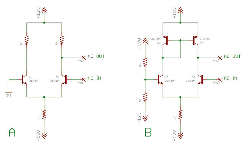
I have two questions about the transistor differential pair shown in the picture above:

1) When used in differential mode with a single-ended input (AC IN) and a single-ended output (AC OUT) is there any advantage to using the current mirror formed by Q6 and Q7 in diagram (B) - or is this just for improving common-mode rejection when using common-mode inputs?

2) When used in differential mode with a single-ended input (AC IN) most schematics show the Base of Q1 (or Q5) to be grounded - is there any advantage to biasing this to approx. 0.6V to get it above Vbe as shown in diagram (B)?

Thanks in advance.
 

1.

Diagram A: Resistor R4 limits output current. (Similar to limitations as found in a typical class A amplifier.)

Diagram B substutes the transistor Q7 for a resistor. The transistor can be turned on to allow greater current flow at the output, and produce wider swings of output voltage.

2.

In Diagram A, the bias leg is automatically more than .6 V above the emitter leg. This is the non-inverting input.

Same with Diagram B.

The addition of the resistor divider makes it easy to shift the output's DC component up and down (within limits).

My knowledge is incomplete so this post may need some correcting.
 

Fig. A is a better way to bias the base of Q1 (and Q5). In Fig B the base current will cause an IR drop across R6 and R9. The DC bias change will be small, but may be important. The drop can be compensated for by putting a resistance equal to R6||R9 in series with the base of Q9 and AC in.

The biggest concern in real opamps would be the noise from base currents. Circuit B will have far more noise because of the base resistors.

The mirror in Circuit B doubles the gain compared to if you had just biased it with a current source. The gain of Circuit B is typically much more than Circuit A because the output impedance of the PNPs is typically much more than R4

rg
 

Status
Not open for further replies.

Similar threads

Part and Inventory Search

Welcome to EDABoard.com

Sponsor

Back
Top