Continue to Site

Welcome to EDAboard.com

Welcome to our site! EDAboard.com is an international Electronics Discussion Forum focused on EDA software, circuits, schematics, books, theory, papers, asic, pld, 8051, DSP, Network, RF, Analog Design, PCB, Service Manuals... and a whole lot more! To participate you need to register. Registration is free. Click here to register now.

Logic of general dynamics of a circuit

yefj

Advanced Member level 4
Joined
Sep 12, 2019
Messages
1,195
Helped
1
Reputation
2
Reaction score
3
Trophy points
38
Activity points
7,217
Hello, i have here a circuit shown bellow it has 4 parts.
part 1 consists of a HEX inverter
https://assets.nexperia.com/documents/data-sheet/74ABT04.pdf

Part2 has some buffer driver with component shown bellow.

https://www.ti.com/lit/ds/symlink/ucc5304.pdf?HQS=dis-mous-null-mousermode-dsf-pf-null-wwe&ts=1701024772623&ref_url=https%3A%2F%2Fwww.mouser.de%2F

Part 3 is a mosfet
https://www.onsemi.com/pdf/datasheet/ndt3055l-d.pdf
https://www.onsemi.com/products/discrete-power-modules/mosfets/NDT3055L#technical-documentation
Part 4 : has a diode connected in a loop

Could you please say the general dynamics of this circuit?
how these parts play together?
Thanks.
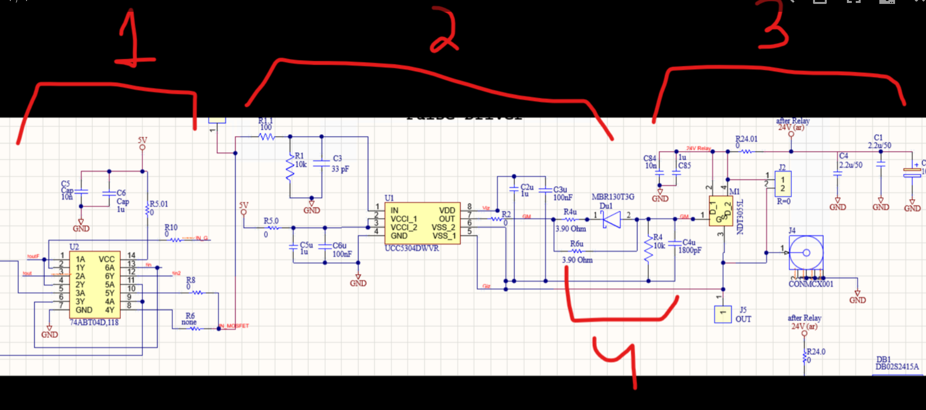
1701030740844.png
 
1. 25 ohm max, 18 ohm typ. per driver. @ 4.5V , lower at 5V.
2. Half-Bridge isolated 3 ohm Pch,2 ohm N Ch + 5 Ohm pullup N Ch @ 12V with dead-time control.
Vdd connection missing.
4. Gate impedance On=3.9 Ω Off= 2 Ω , Cg= 1800 pF+Ciss=180 pF= QV , T=RC, Faster turn Off
3. Nch FET 100 mΩ max @25'C + 24V decoupling caps

Why do you need an isolated driver with common grounds?
Why do you need deadtime half-bridge to drive a single Nch FET?

Low quality schematic.
 
Even with Vdd connection, the isolated gate driver doesn't work in this MOSFET configuration. It would need a floating power supply on top of OUT node.
 
I suspect this only shows the top side of a half bridge with the OUT to load also controlled by a similar circuit with a floating +15V supply where the Vdd of U1 missing the + 15V (20V max) while the low side uses the same 15V to Vdd.

There is also some 24V shown which exceeds the Vdd rating of U1.

Needs some more effort to work. Now my questions in #1 are answered if my assumptions are correct.
U1 has internal deadtime control, while R+RD//C in section 4 provide external deadtime control to the HV FETs.

The hidden low side cct. must be PWM in order to pump Cboot to Rboot and diode to create Vboot.
But Vdd on U1 is still missing It will be 14V above Vdd=15V on hidden low side isolated driver which uses PWM to pump high side which has Vdd= Vboot, Vss=out and low side uses Vdd=15V, Vss=0V (isolated)
1701045093203.png
 
Last edited:
Hello Stewart , its supposed to output threw the mosfet of section 4 an RF signal as a pulse.
mosfwet is a switch which needs a pulse itself on the gate to output the pulse rf_signal.
1.How does the pulse for the mosfet is being created?
2.how does the RF-signal for the mosfet is being created?
3.how are they combining in the mosfet?
Thanks.
 
We see a single high-side switch, not necessarily pwm operated. The coaxial jack suggests it's sending pulses to a load.
The driver supply is missing or "hidden". Bootstrap supply would involve restrictions for output waveforms and load characteristic, I don't see it as general acceptable solution.
 
Hello, Stewart,thank you for the insight.regarding the circuit:
maybe the hex invertor is creating the pulse signal for the mosfet?
could you please say how with hex inverter we can create one?

Thanks.
 
Hello, Stewart,thank you for the insight.regarding the circuit:
maybe the hex invertor is creating the pulse signal for the mosfet?
could you please say how with hex inverter we can create one?

Thanks.
I created /modelled one inverter. Did you not recognize it in your other Q??

I don't know what you don't know and your question is vague.
 
Hello Stewart ,Yes i understand that my schematics is partial.
Could you please recommend me a god manual on the half bridge so i could learn its parts and simulate them ?
especially if you have a manual for a schematics shown below this is exactly the structure i got, and i'll be glad to learn about it.
Thanks.
1701503360953.png
 
Last edited:
Hello, what is the logic of this part before the mosfet?
I know its for faster discharge, but there are three resistors.
Thanks.

1711104613781.png
 
Last edited:
Hi,

They have different names. For a reason.

R_ON for defining switch_ON_timing
R_OFF for defining switch_OFF_timing
R_GS .. to pull down V_GS ... to ensure safe OFF when not powered

Klaus
 
Each of the 4 cascaded MOS switches ( 3 shown) has some asymmetric delay time and power loss during switching with some reduction in RdsOn but increase in Ciss.

Balancing these with shootthru power and conduction ON power can be a difficult design when thermal effects are included and variations in Vth of each FET. The diode current and thus incremental resistance depends on the gate ESR from internal and external capacitance. These are dynamic SOA concerns and also affect nonlinear effects including odd mode oscillations that depend on shunt load.

Making the models reflect the real parts and optimal layout parasitics is your challenge to simulate the best system performance.

This is a crude 1st order simulation.


Can you imagine the effects of power dissipation, delay time and transition impedance will be in the next stage? I can't .

Not with what has been given, nor do I know what is your design spec or optimal design.

Break each stage down into specs then determine the dependent variables and choose the optimal FETs for Ciss*Rg, Coss*RdsOn FETs for your load voltage and current or similar parameters that affect thermal losses and power transfer from PDN to gate trigger to load.

Your best bet is to learn from experts and use App notes or a similar production design. IDK.
 
Last edited:

LaTeX Commands Quick-Menu:

Part and Inventory Search

Welcome to EDABoard.com

Sponsor

Back
Top