Continue to Site

Welcome to EDAboard.com

Welcome to our site! EDAboard.com is an international Electronics Discussion Forum focused on EDA software, circuits, schematics, books, theory, papers, asic, pld, 8051, DSP, Network, RF, Analog Design, PCB, Service Manuals... and a whole lot more! To participate you need to register. Registration is free. Click here to register now.

Logic Circuit and Carry Save Adders

Status
Not open for further replies.

mahaju

Full Member level 2
Joined
Mar 17, 2007
Messages
125
Helped
7
Reputation
14
Reaction score
2
Trophy points
1,298
Activity points
2,252
Hi

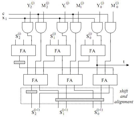
If a number is in carry save notation how do I shift it?
A number in normal binary notation when shifted right, would cause the LSB to go out of the number and the MSB to be padded with zero or the sign bit

But if the number is in redundant Carry-Save format, how do I shift it?

I desperately need help in this
I have been trying to look for this since quite a few days and non of the forums are helping me in any way

Thanks in advance
 

You would simply shift the carry and the save vectors each right by one. Doing this and then summing to convert the carry and save vectors into one sum will have the same effect as converting first and then shifting. The difference is that you would need two shift registers for the method you are talking about. If you summed the two before doing the shift you would need another full adder and one shift register. There may be a benefit of the former approach is if the rest of the circuit (or in your case, embedded system) can utilize the carry and save vectors more efficiently than a single sum vector.
 

Hi
Thanks for your reply
Here is a circuit implementation of shifting of numbers in Carry Save format but I don't quite understand how this is supposed to shift the number
I believe the shifted version is still in the carry save format but I don't understand how it works
Here is a brief explanation of what this circuit is supposed to do:

first it multiplies the bit Xi to the 3-bit number {Y2 Y1 Y0} and adds this to another 3 bit number {S2 S1 S0} where the number S is in Carry Save form
The result of this addition is also in Carry Save form (the result from the upper row of FA)
If the LSB of this result (the bit 't') is 1, the bit 'c' is asserted to 1 and the number {M2 M1 M0} is added to the result of the first row of FA
One thing I don't understand is that why is the Carry output of the leftmost FA of the first row of FA entered into the right most FA of the 2nd row (the shaded box represents flip flops to cause delay I think)

The other thing I don't understand is the arrangement of the output of the 2nd row of FA. Ultimately what this circuit is supposed to do is add Y(if Xi is 1; this is also apparent from the figure as Xi has been ANDed with each bit of Y), S and M(depending on the value of c, which depends on the value of t). The result of the addition (the output of the 2nd row of FA) should also be shifted right by 1 bit. How does this figure correspond with the right shift? Do you have any ideas? I desperately need help with this so if you have any ideas please share them with me.

Thanks

Have a nice day :lol:


Status
Not open for further replies.

Part and Inventory Search

Welcome to EDABoard.com

Sponsor

Back
Top