Continue to Site

Welcome to EDAboard.com

Welcome to our site! EDAboard.com is an international Electronics Discussion Forum focused on EDA software, circuits, schematics, books, theory, papers, asic, pld, 8051, DSP, Network, RF, Analog Design, PCB, Service Manuals... and a whole lot more! To participate you need to register. Registration is free. Click here to register now.

LM311 comparator input from Colpitts oscillator questions

NigthMoth

Junior Member level 3
Joined
Aug 28, 2023
Messages
29
Helped
0
Reputation
0
Reaction score
6
Trophy points
3
Activity points
502
Hello all

I was studying how to use comparators, so decided to feed LM311P comparator with 10kHz sinusoidal waveform generated by Colpitts oscillator to confirm the comparator behaviour. But (as you've probably already guessed) LM311P didn't behave as I expected (and Colpitts oscillator as well).

Here is what I've done, and questions at the end of this post:

Colpitts oscillator design for10kHz ~5Vpp oscillations

Actually I don't know how to estimate Colpitts oscillations Vpp, so decided to set power supply as +5V

Transistor biasing:
- R1, R2, Rc, Re for voltage divider configuration bias selected so @Vcc = 5V, Ic~=1mA, Vce~=0.5*Vcc;
- Ce selected so X_Ce @10kHz < 0.1*Re => Ce > 0.34uF, 0.47uF is OK;
- Cin selected so X_Cin @10kHz < 0.1*(R1||R2) => Cin > 0.69uF, 10uF is OK;
- Cout selected so X_Cout @10kHz < 0.1*Rload and Rload will be at least 10xRc => Cout > 0.009uF, 47uF is OK;
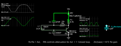
Tank circuit
C = C1*C2/(C1+C2) ~= 0.025uF;
f = 1/[2*pi*sqrt(L1*C)] ~=10.1kHz;

I estimated Av for this confirguration as described here
r'e ~= 25mV/Ie = 25mV/1mA = 25 Ohm
Av ~= Rc/r'e = 1800Ohm/25Ohm = 72
Criterion for oscillations to start from as described here:
beta = C1/C2 = 0.082 and 1/beta = 12
72 >= 12 so Av >= 1/beta so it is ok for oscillations

and

According to Datasheet
- Vcc(min) = 3.5V - OK, my Vcc is 5V
- Vi(min) = Vcc- +0.5V = 0+0.5V= 0.5V - OK, expected Vin(min) is 1.43V, minimum of sin wave from Colpitts oscillator Setup 1
- Vi(max) = Vcc+ -1.5V = 5-1.5V= 3.5V - OK, expected Vin(max) is 2.76V, maximum of sin wave from Colpitts oscillator Setup 1
- Icc+(max) = 7.5mA - OK, R3 = 2.7kOhm to ensure supply current <7.5mA
(I have +5V and +18V power supply, I'm affraid to use +18V by mistake, so select 2.7k resistor)

Here is what I got:

Setup 1: Colpitts oscillator - OK, but frequency is not as I expected
Setup 1 circuit.png

Setup 1: Circuit diagram​
изображение_2024-01-04_233652245.png

Setup 1: Realisation​
Setup 1 Colpitts Test 1.jpg

Setup 1: Test​

Setup 2: Colpitts oscillator & LM311P (Emitter output) - OK, but output voltage less than expected
Setup 3 circuit.png

Setup 2: Circuit diagram​
изображение_2024-01-04_234121151.png

Setup 2: Realisation​
Setup 3 Colpitts and LM311 emitter Test 1.jpg

Setup 2: Test​

Setup 3: Colpitts oscillator & LM311P (Collector output) - Fail
Setup 4 circuit.png

Setup 3: Circuit diagram​
изображение_2024-01-04_234529749.png

Setup 3: Realisation​
Setup 4 Colpitts and LM311 collector Test 1.jpg

Setup 3: Test​

My questions:

1) Colpitts oscillator frequency question (Setup 1)

I was trying to setup 10kHz frequency for Colpitts oscillator
I checked values for C1,C2 and L1 in tank circuit with RLC meter and they almost as specified (within +/-5%)
But I got 13.69kHz instead of ~10kHz.
And i cant figure out why?

My first guess was that my Lchoke inductivity is too high, and, as I undersand, It appears in parallel with C1 in AC equivalent circuit,
so tank circuit becomes more complicated?
And, for example, if I substitute (L1||Lchoke) = 5mH into tank circuit equation i get 14kHz, almost as 13.69kHz measured with oscilloscope.

When I simulate this oscillator with Micro-Cap 12, I got ~11.7kHz
It is as close to 10kHz (expected) as to 13.69kHz (received), so I'm confused..

Also, if Lchoke < 10mH, there is no oscillations. I picked up 10mH value manually, not by calculation.


2) Question regarding "Emitter output" from LM311P (Setup 2)
Almost as I expected, but why amplitude of square wave is only +2.24V but not ~Vcc(+5V)?


3) Question egarding "Collector output" from LM311P (Setup 3)
Why there is no square wave from comparator's collector output regardless of Pot1 referrence voltage in my Setup 3?
It works rather like some kind of flip-flop: always LOW when Vref(IN-) <0.22V and always HIGH when Vref(IN-) >0.22V,
even if IN+ is a sinusoid oscillating from 1.86V to 3.86V.
 
Hi,

LM311 is a comparator - as you already mentioned.
But you used it like an OPAMP with external gain setup of +1.

--> Don´t use a comparator this way.
An OPAMP is no comparator and a comparator is no OPAMP. Both are designed for completely different operation modes.
Sadly they share the same schematic symbol. And also sadly many tinkerers and hobbyists use them wrongly. Thus there are many wrong schematics in the inernet.

Please read the datasheet and other related documents provided by the manufacturer.

Klaus
 
As already mentioned, buffer IC1 input has no DC bias, resulting in unstable operation. You can e.g. omit Cin to get defined bias. Comparator LM311 has unsuitable Vcc series resistor R4, not suggested in any manufacturer application.

I don't see that the circuit tries to use LM311 as opamp.
 
1) Do you have a R4 in series with LM311 + supply pin ? That should be removed.

2) To get square wave the bias point pf LM311 has to be set to halfway between sine peak
to sine min.


Regards, Dana.
 
Hello All!

Taking into accout received recommendations, I modified my circuit:
- Unbiased opamp buffer has been replaced with single supply biased Av=1 inverting amplifier
(I didn't found how to correctly bias single supply simple voltage follower,
so I used single supply biased Av=1 inverting amplifier as described in article Avoiding Op Amp Instability Problems In Single-Supply Applications);
- resistor in series with LM311P's power supply has been removed
(It looks like I misread LM311 datasheet. In "electrical characteristics" table I saw that Icc+(max) is 7.5mA and I tried to limit Icc current with
that resistor, but it was for "Supply current from VCC+, output low", not for device absolute maximum rating)
- Tried to keep LM311P refference voltage halfway between sine peak to sine min;
- Colpitt's output capacitor removed;

There is new circuit diagramm:
Schematic 6_2.jpg


But my problem still not solved: Comparator's "Collector output" configuration still not work.
Comparator's Collector Output (CH2 in my diagramm) is always a strait line (DC voltage) about 0.4...0.9Vdc independently of refference voltage
at inverting input of the comparator.
Here is picture:
Setup 6c.jpg


I was able to change comparator's collector output Vdc level not by rotating potentiometer shaft, but by changing value of pullup resistor R3:
Output was about 2.5V with R3 = 120...220 Ohm, and it was about 5V for R<51 Ohm. But there wasn't square wave at all.
Also I tried to make comparator's supply voltage +18V, but there was not any effect.
Moreover, I tried to replace LM311P comparator chip with four another LM311P chips, but all those chips has the same behaviour.

From the other side, "Emitter output" confirguration works well.
Here is picture for "Emitter output":
Setup 6e.jpg


So, for this moment, I decided to not rely on "Collector output" of LM311P comparator in future and use only "Emitter output" for my projects.
And I considering these possibilities why my LM311P "Collector output" doesn't work:
- I'm still not getting how to use comparator's "Collector output";
- I was unlucky enough to make my circuit parameters to be somehow incompatible with LM311P internal circuity;
- All five LM311P chips in my inventory are bad;
 
Hi,

I did not go deep into the posts ....

What I´ve noticed (referring to your post#8)
* the waveform on the scope for emitter output is way too slow in rise and fall.
* you say "STRB (pin5)" --> but it is pin#6
* you say "BAL(pin6)" --> but it is pin#5
* you say: "pin#5 and pin#6 shorted together" --> but datasheet says: "all characteristics are measured with BALANCE and BAL/STRB open"
* don´t use a that (unsuitbale) high ohmic pot at comparator input. It makes it sesitive to capacitove effects. --> add a capacitor to GND at the pot_center.

* Pictures in post#1 seem to show a resistor on pin#5 to VCC
* pictures in post#1 show that you randomly use upper and lower GND and VCC colums on your bread board. Don´t do this. Always refer to one column. Put a capacitor between VCC and GND.

Klaus
 
When doing collector output you sure you have the emitter grounded ?

You are single supply, 5V, common mode range is (+/- 15V supplies)

1704801370791.png


So worst case its .5V off negative rail and 2V off positive rail, for a range of 2.5V or .5 to 3V. Again this
is at +/- 15v supply, but would not scale 1:1 with change in it. Unfortunately datasheet does not show
CMR versus supply.

And this :

1704801751759.png


Regards, Dana.
 
Last edited:
Hi,

I did not go deep into the posts ....

What I´ve noticed (referring to your post#8)
* the waveform on the scope for emitter output is way too slow in rise and fall.
* you say "STRB (pin5)" --> but it is pin#6
* you say "BAL(pin6)" --> but it is pin#5
* you say: "pin#5 and pin#6 shorted together" --> but datasheet says: "all characteristics are measured with BALANCE and BAL/STRB open"
* don´t use a that (unsuitbale) high ohmic pot at comparator input. It makes it sesitive to capacitove effects. --> add a capacitor to GND at the pot_center.

* Pictures in post#1 seem to show a resistor on pin#5 to VCC
* pictures in post#1 show that you randomly use upper and lower GND and VCC colums on your bread board. Don´t do this. Always refer to one column. Put a capacitor between VCC and GND.

Klaus
Thank you for suggestions for adding capacitor to pot and breadbord rails. Noted for future projects.
As for "pin#5 and pin#6 shorted together", I shorted them because I saw this note in Datasheet under pic 12
изображение_2024-01-09_214456913.png

Actually I tried to leave pin 5 and pin 6 unconnected, but that also didn't help
--- Updated ---

So worst case its .5V off negative rail and 2V off positive rail, for a range of 2.5V or .5 to 3V. Again this
is at +/- 15v supply, but would not scale 1:1 with change in it. Unfortunately datasheet does not show
CMR versus supply.
Thank you, maybe this is the key. I'll try to modify my circuit so oscillations feed to comparator will fit into this window
 
Last edited:
Hi,

My datasheet tells something different.
Thus you see how urgent it is to post a link to your datasheet, so we can talk about the same document.

In my datasheet it´s "Figure 17. Offset Balancing"
it says: "If offset balancing is not used, the BALANCE and BAL/STRB pins must be unconnected. It is also acceptable to short
pins together."

A wonderfully clear information: "they MUST be unconnected" ... or can be tied together ;-)

It also says: "Do not connect strobe pin directly to ground, because the output is turned off whenever current is pulled from the
strobe pin."

****
My opinion:
There is a problem with your circuit.
So if you want the problem to be solved yo need to show us your exact circuit.

Please post a couple of photos (JPG, max 300k each) so we can see al details of your circuit. Wiring, parts, part markings, color rings on resistors...
In short: all informations that we can build the very same circuit as you have.. to make our own tests here.

Klaus
 
Please post a couple of photos (JPG, max 300k each) so we can see al details of your circuit. Wiring, parts, part markings, color rings on resistors...
In short: all informations that we can build the very same circuit as you have.. to make our own tests here.

Thank you all for your time checking my circuits
Here is pictures of my circuit and breadboard layout i used, so anyone can build the same

Breadboard layout
LM311_Test_06_BB_01.png


Real bredboard
изображение_2024-01-09_231908151.png


Full setup including power supply (From laptop usb) and oscilloscope
изображение_2024-01-09_231946093.png
 
On your breadboard drawing I dont see where you coupled your upper buss bar GND witht he lower buss bar GND ?

Careful using those breadboards, I have done moderate fast circuits in them but contacts to components
always a challenge. The mechanical female part of connection seems to get poor performance ver time.

The bypass caps, .1 uF, Ceramic disks ? When you are doing bypassing ESR matters :

1704815046950.png


Regards, Dana.
 
On your breadboard drawing I dont see where you coupled your upper buss bar GND witht he lower buss bar GND ?

Careful using those breadboards, I have done moderate fast circuits in them but contacts to components
always a challenge. The mechanical female part of connection seems to get poor performance ver time.

The bypass caps, .1 uF, Ceramic disks ? When you are doing bypassing ESR matters :

View attachment 187674


Regards, Dana.
+5V and GND for both pair of rails provided by breadboard power supply module that i bought together with breadboard.
Sorry, I didnt show this supply module on drawing.

Bypass 0.1uF capacitors are Polyester film type.
Thank you for bringing this aspect to my attention, i'll add to my notes
 
Hi,

I can not see the markings of the ICs. I mean in the photos of the real circuit... not the breadboard image.
And still the link to your datasheet is missing.

Klaus
 
Define you goals to achieve and avoid. (Specs)
My goal for this project is to get square wave from LM311's collector output. Conditions: +5V power supply, Sin wave input from available Colpitt's oscillator.
OR, if it is impossible, my goal is to know why it is impossible. Square wave or uderstanding what was wrong, there is no practical purpose, it is for learning.
--- Updated ---

Hi,

I can not see the markings of the ICs. I mean in the photos of the real circuit... not the breadboard image.
And still the link to your datasheet is missing.

Klaus
There are pictures:
LM358P
изображение_2024-01-10_003911167.png


LM311P
изображение_2024-01-10_004018367.png


As for LM311 Datasheet: Sorry, I can't find exactly link I downloaded it before, so I'm attaching pdf file from my computer I'm reffering to.
 

Attachments

  • Data Sheet LM311 (Comparator) LM111, LM211, LM311.PDF
    511.6 KB · Views: 44
Last edited:
Hi,
As for LM311 Datasheet: Sorry, I can't find exactly link I downloaded it before, so I'm attaching pdf file from my computer I'm reffering to.
Why using mature datasheets?

It´s TI, they have an internet site, they provide the datasheets. It´s the most reliable and most up to date source.

Klaus
 
Using BJT Op Amps and Comparator inputs can be NPN, PNP or JFET. These are PNP so you must avoid signals with 2 diode drops + IR drop or 2V at -40'C where Vpn-jcn is greatest. This caused your open collector comparator to fail because the Op Amp out Bias was too high for comparator input and open collector with pullup has more V gain. Yet it is possible to make both work by reducing bias. For a Colpitts Osc (basic) the signal must be Vpp between 1/3 and 2/3 of Vcc, no more , no less. *unless you design 2 diode limiter* then it will work over a wide Vcc range like 1.5 to 12V.

1704828279334.png


When your NPN is saturated the collector has a flat bottom (low Vce) and this asymmetry will skew your duty cycle when squaring up with high gain on your last stage.

When the Vcollector rises to maximum, this is due to lower Ic current and hFE is also reducing due to a drop in Vbe, giving as more rounded +ve peak.
All single stage harmonic distortion is due to this effect (2nd order harmonics) when there is no negative feedback. Sharp clipping causes odd harmonics when square and both even & odd harmonics when the duty cycle is very narrow.

Fortunately , the Colpitts Osc. uses negative feedback for AC and you can also use it for DC feedback by eliminating one capacitor. So this improves the sine quality. But when the gain is too high the feedback resistor becomes far too sensitive to find that closed loop gain just a hair above unity (=1).

So we start the design by reducing the open loop gain using Rc/Re without any bypass and gain of 20 or perhaps Rc/Re = 50 then reduce this ratio depending on hFE.
We expect hFE range > +/-50% to 3:1 for max:min ratio is possible and must be tolerated. This is a manufacturing mass production limitation, unless binned for ($) tighter tolerances done by some suppliers on some transistors. (e.g. Rohm)

Sine Wave Design Specs

  1. Vcc= 5V 10%
  2. Freq. = 10 kHz 10% (do we care?)
  3. Current= Let's say 1 mA, can easily be more.
  4. Distortion < 10 %, Can be tweaked to 1% or 0.1%
  5. Open loop gain , let Rc/Re be >20 < 50
  6. Vsine = < 30% to 60% max of 5V = 1.5 to 3Vpp max ( lower is better to reduce distortion, higher is guaranteed to oscillate but more distorted)
  7. Vcm to next stage must be < 3Vpeak and if Vce < 100 mV @ 1mA it is saturated. We can AC couple or DC couple if we can.
  8. which means collector DC bias must be to <1.6V , preferably 1V to permit a larger swing and avoid the 2V CM headroom need for the PNP inputs. Then we'll try to reduce swing towards 50% of Vcc where is is more symmetrical with the gain just slightly above unity (1). (With A soft clamp we can make this more tolerant to regulate distortion from excess hFE gain.

Yet for any linear oscillator the Barkhausen Criteria for instability or clean sine waves the closed loop gain is determined by the amount feedback gain used to reduce the open loop gain. So reducing Rfb from Collector to Base will increase the bias current, Ib and Ic and thus increase gain while input base impedance provides the voltage divider at base for negative feedback. Normally for an Op Amp Av= -Rfb/Rin. For a very low gain common emitter it's about 50% of this ratio.

So I end up with this simulation. With Vdc out avg = 1V and 1.82 Vpp ac

1704831021652.png


Now I see the frequency is pretty close but then 10mH is likely 10%. Vpp meets spec, Vdc at collector is almost 1V avg also meets spec and f= 10.1 kHz. We could tune it by adding ~ 0.3% of Cb between Cc and Cb which is in parallel with the Coil self-capacitance, due to SRF or self resonant frequency of the coil. So "your mileage/value will vary."

Notice I moved Cc (closest to the collector) from ground to Vcc. Does it matter? No. Supply is very low impedance relative to the cap at 10 kHz. So it is equivalent to an AC gnd.

Now we really don't need an Op Amp any more unless you wanted to buffer it with unity gain. I didn't need it.

Design Specs for Limiter
  1. Vo = 5V +0/- 5%, 0 to 150 mV
  2. T rise time << 1% of 10 kHz cycle or 1 us
  3. Input impedance >= 50 x source impedance or >= 50 kohm
  4. Vio input offset < 10 mV
  5. Power = 1 ~ 2 mA @ 5V nominal
  6. Startup time < 10 ms to steady state.

Using Pullup on collector of 1k to 5V draws 1 mA more and can tolerate RC~ 1us for C(load) <= 1 us/ 1 k = 1 nF which is OK for now.
So use 1k pullup unless the spec changes.

Let's choose ~100 cycles is easy to filter some ripple or T ~ 10 ms, Use DC (from LPF filtered sine) with 100k and non-inverting input uses 100k we are DC coupled yet comparing AC zero-crossings. Steady state is approx 10 * Tau so if RC = 1ms , R=100k, then C= 100 nF ripple should be ~ -40 dB which is a good tradeoff for fast start and low ripple.

Then I get this simulation. It's not perfect, but close enough for gov't work!

1704832194539.png


But if I just had some CD4000 series inverting gate CMOS around from the '70's, I could do this. The far left R has almost zero effect on RC integrator Oscillator and is slightly more reliable than Schmitt Trigger Oscillators, which also work.

1704833101854.png


Bottom line is Colpitts Osc needs extra effort to run clean with a wide tolerance to hFE. Otherwise it's the pits and there are much better designs.
But your only problem was not understanding the datasheet schematic or the IC specs for Vcm and the headroom to avoid hitting your head on. But very nice schematic with notes. 10/10
 

Attachments

  • 1704830511655.png
    1704830511655.png
    107 KB · Views: 35
Last edited:

LaTeX Commands Quick-Menu:

Similar threads

Part and Inventory Search

Welcome to EDABoard.com

Sponsor

Back
Top