Continue to Site

Welcome to EDAboard.com

Welcome to our site! EDAboard.com is an international Electronics Discussion Forum focused on EDA software, circuits, schematics, books, theory, papers, asic, pld, 8051, DSP, Network, RF, Analog Design, PCB, Service Manuals... and a whole lot more! To participate you need to register. Registration is free. Click here to register now.

Vdd/Vcc noise, slow rise time CMOS input impact

danadakk

Advanced Member level 6
Joined
Mar 26, 2018
Messages
3,095
Helped
414
Reputation
848
Reaction score
723
Trophy points
113
Activity points
13,429
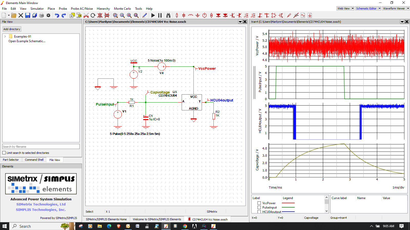
100 mV RMS on Vcc, coupled with slow rise time CMOS inputs, lots of output jitter -
1711026492884.png


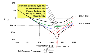
Bypass capacitor ESR crucial, as well as Tr, Tf of the applicable input/gate.


1711028335438.png


Regards, Dana.


Regards, Dana.
 
One can also see the open loop voltage gain from the above noise sensitivity test.
1711051164751.png


We often take for granted that computers with billions of logic transitions per second never have logic errors ( that we know of). This can be predicted by using the clipped waveforms of logic with a known relationship SNR vs BER log curve. If a 40 dB SNR translates into a bit error rate (BER) of 10e-12, that is not good enough for computer logic at Tera-flop speeds. It might improve an order of magnitude per 1dB in SNR. However non-linear noise often becomes more significant than Gaussian Noise.

As Dana has well-demonstrated here is that 5V/100mV rms or 50:1 or 34 dB is a certainly problem. Sometimes SNR is expressed as p-p jitter and there are conversion factors for rms to p-p random and non-random noise.


PSU filtering IC decoupling must never be taken for granted as the rejection ratio of supply noise must be fully understood in SNR terms and how this translates into future errors. Each Gate has a crossover change in shootthru current Ron*Coss that draws current from both Vdd &Vss using the bypass cap ESR*C to attenuate the injected noise. a 0.1 uF cap might have an ESR of 5 Ohms or 0.5 Ohms, which values you choose for C and ESR depends on the size of the IC to improve the otherwise injected low SNR onto the supply. It can be modeled as an RC to RC attenuator with Vdd pp noise with spectral risetimes to determine the BW=0.35/Tr.

For measuring PSU noise on logic, as a former Test Engineer, I would prefer to use a cap on board from Vdd to a 50 Ohm coax to a spectrum analyzer or DSO terminated with 50 Ohms.

Is 50 dB SNR good enough or 60 dB? or ?? on Logic supply and ground noise? I'll let you think about rise times and supply noise sensitivity.
 
Last edited:

LaTeX Commands Quick-Menu:

Part and Inventory Search

Welcome to EDABoard.com

Sponsor

Back
Top