Continue to Site

Welcome to EDAboard.com

Welcome to our site! EDAboard.com is an international Electronics Discussion Forum focused on EDA software, circuits, schematics, books, theory, papers, asic, pld, 8051, DSP, Network, RF, Analog Design, PCB, Service Manuals... and a whole lot more! To participate you need to register. Registration is free. Click here to register now.

LDO - transient accuracy

Status
Not open for further replies.

massive_attack

Newbie level 6
Joined
Jan 4, 2008
Messages
11
Helped
0
Reputation
0
Reaction score
0
Trophy points
1,281
Activity points
1,346
hola!

I'd like to ask you about transient response of LDO.

typically it looks like this


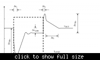
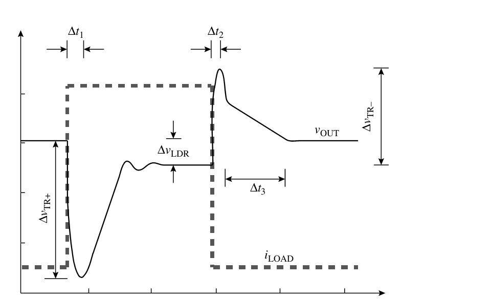
I'm considering time \[\delta\]t3 . It's related to Cout slewing by feedback resistors or another sink.
The thing that in my simple design which is simple two stage opamp + pmos device this time is not shorter when I use 10x smaller resistors.
In the test bench I use worst case situation loading from 0 to Imax and back to 0 (tr,tf =1ns) with ESR=0(which is not true normally).

GBW of the system is 500kHz, PM > 70deg

What can be the reason of such long time? Should i worry that ? The output is about 70mV higher than should be.

regards
 

what kind of compensation did you used? the slew rate could be related to the compensation network.
 

I use basic Cout + ESR compensation which is enough in this situation.
 

What can be the reason of such long time?
Such an LDO can only source current, but not sink it, hence this slow decay.
If you really need it faster, you'd have to add a small controlled sink transistor.

Should i worry that ?
Depends on the application. Ask your customers!

The output is about 70mV higher than should be.
If absolute accuracy is important, Vref trimming should be considered.
 

70mV difference is due to limited load regulation / finite output impedance. With two stage LDO, you can only try to increase the dc loop gain to reduce it most often at the cost of the moving the cut-off point in the load regulation characteristic to low frequencies.
 

writting 70mV i meant overshoot, which SLOWLY (100us) relaxes to proper output voltage at 1mA. It's even worse when load falls to 1u.

Another serious thing which i met is startup after turning on enable pin. Output voltage rises almost to vin and settles after 150us. The problem is that during the startup, PMOS device sources 3A!
how to prevent it, what kind of ciurcuit should i use.
any working examples ?

regards
 

writting 70mV i meant overshoot, which SLOWLY (100us) relaxes to proper output voltage at 1mA. It's even worse when load falls to 1u.
Quite clear, s. my posting above!

Output voltage rises almost to vin and settles after 150us. The problem is that during the startup, PMOS device sources 3A!
I = C * δV/δt . You load 150µF to 3V ?

how to prevent it
Does it hurt? If so: lower output cap -- or a soft start mechanism.
 

Status
Not open for further replies.

Part and Inventory Search

Welcome to EDABoard.com

Sponsor

Back
Top